|
|
|
| DS33Z41 Quad IMUX Ethernet Mapper |
|
|
|
|
|
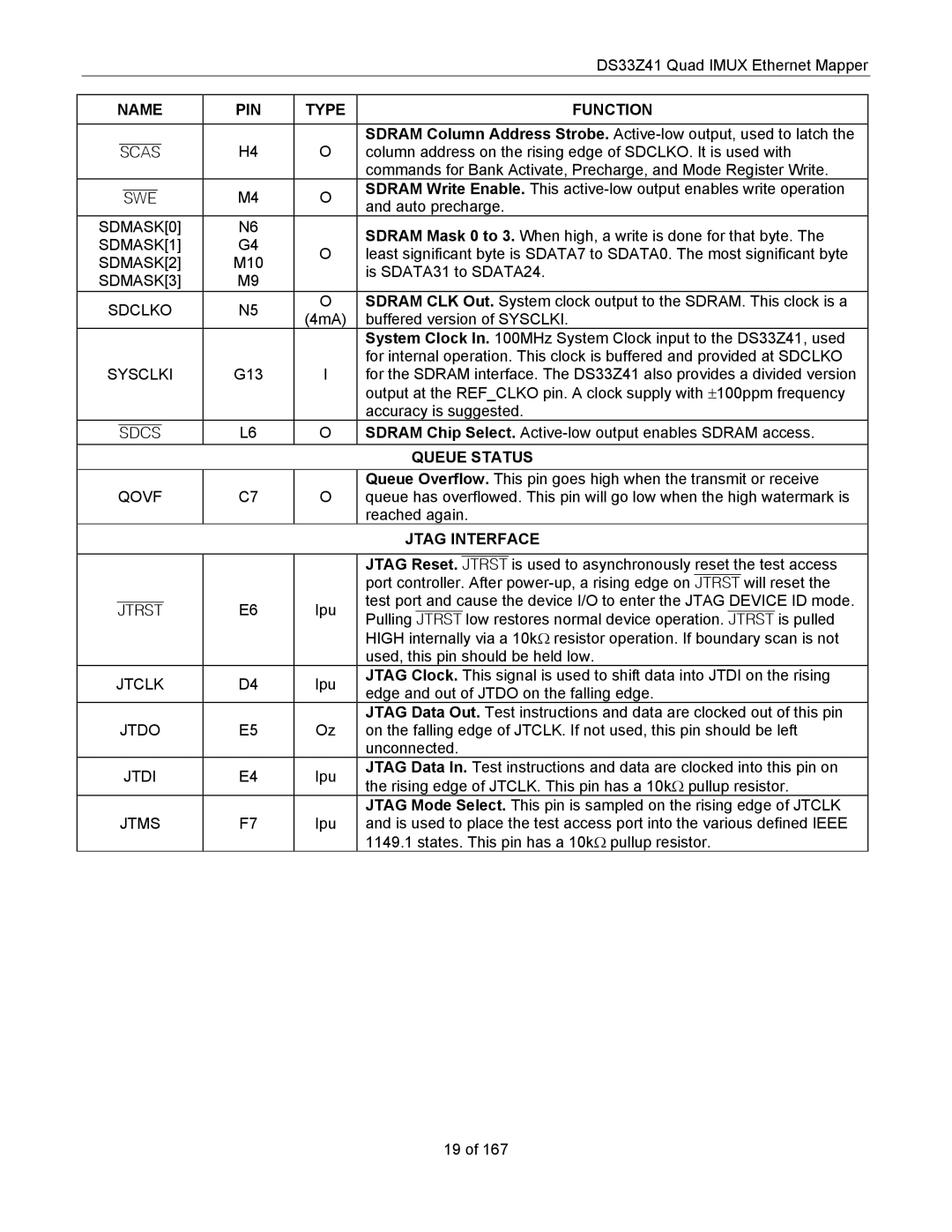
| NAME | PIN | TYPE | FUNCTION |
|
|
|
|
|
|
| H4 | O | SDRAM Column Address Strobe. |
| SCAS | column address on the rising edge of SDCLKO. It is used with | ||
|
|
|
| commands for Bank Activate, Precharge, and Mode Register Write. |
| SWE | M4 | O | SDRAM Write Enable. This |
| and auto precharge. | |||
|
|
|
| |
| SDMASK[0] | N6 |
| SDRAM Mask 0 to 3. When high, a write is done for that byte. The |
| SDMASK[1] | G4 |
| |
| O | least significant byte is SDATA7 to SDATA0. The most significant byte | ||
| SDMASK[2] | M10 | ||
|
| is SDATA31 to SDATA24. | ||
| SDMASK[3] | M9 |
| |
|
|
| ||
| SDCLKO | N5 | O | SDRAM CLK Out. System clock output to the SDRAM. This clock is a |
| (4mA) | buffered version of SYSCLKI. | ||
|
|
| ||
|
|
|
| System Clock In. 100MHz System Clock input to the DS33Z41, used |
|
|
|
| for internal operation. This clock is buffered and provided at SDCLKO |
| SYSCLKI | G13 | I | for the SDRAM interface. The DS33Z41 also provides a divided version |
|
|
|
| output at the REF_CLKO pin. A clock supply with ±100ppm frequency |
|
|
|
| accuracy is suggested. |
| SDCS | L6 | O | SDRAM Chip Select. |
|
|
|
| QUEUE STATUS |
|
|
|
| Queue Overflow. This pin goes high when the transmit or receive |
| QOVF | C7 | O | queue has overflowed. This pin will go low when the high watermark is |
|
|
|
| reached again. |
|
|
|
| JTAG INTERFACE |
|
|
|
|
|
|
|
|
| JTAG Reset. JTRST is used to asynchronously reset the test access |
|
|
|
| port controller. After |
| JTRST | E6 | Ipu | test port and cause the device I/O to enter the JTAG DEVICE ID mode. |
| Pulling JTRST low restores normal device operation. JTRST is pulled | |||
|
|
|
| |
|
|
|
| HIGH internally via a 10kΩ resistor operation. If boundary scan is not |
|
|
|
| used, this pin should be held low. |
| JTCLK | D4 | Ipu | JTAG Clock. This signal is used to shift data into JTDI on the rising |
| edge and out of JTDO on the falling edge. | |||
|
|
|
| |
| JTDO | E5 | Oz | JTAG Data Out. Test instructions and data are clocked out of this pin |
| on the falling edge of JTCLK. If not used, this pin should be left | |||
|
|
|
| unconnected. |
| JTDI | E4 | Ipu | JTAG Data In. Test instructions and data are clocked into this pin on |
| the rising edge of JTCLK. This pin has a 10kΩ pullup resistor. | |||
|
|
|
| |
|
|
|
| JTAG Mode Select. This pin is sampled on the rising edge of JTCLK |
| JTMS | F7 | Ipu | and is used to place the test access port into the various defined IEEE |
|
|
|
| 1149.1 states. This pin has a 10kΩ pullup resistor. |
19 of 167