S1D13705
Document No. X27A-Q-001-04
This page Left Blank
Customer Support Information
This page Left Blank
S1D13705 Embedded Memory LCD Controller
February
Software Suspend mode LCD power-down sequencing
Embedded 80K byte Sram display buffer
Hardware Functional Specification
Document Number X27A-A-001-10
This page Left Blank
Table of Contents
SwivelView
Power Save Modes
Registers
Mechanical Data
List of Tables
This page Left Blank
List of Figures
2 Bit-per-pixel Monochrome Mode Data Output Path
Introduction
Scope
Overview Description
CPU Interface
Features
Integrated Frame Buffer
Display Support
Miscellaneous
Display Modes
Clock Source
Package
Typical System Implementation Diagrams
Typical System Diagram SH-4 Bus
Typical System Diagram M68K #1 Bus
Typical System Diagram Generic #1 Bus
Host Interface
Functional Block Diagram
Functional Block Descriptions
Memory Controller
Look-Up Table
Power Save
Power Save contains the power save mode circuitry
LCD Interface
Pins
Pinout Diagram
Package type 80 pin surface mount QFP14
Pin Names Type Pin # Cell
Pin Description
Key
Description
For MC68K #1, this pin inputs the R/W# signal
For SH-3/SH-4 mode, this pin inputs the write enable signal
Input This pin inputs the chip select signal
For the lower data byte WE0#
Pin Name Type Pin # Cell
Miscellaneous
Power Supply
Clock Input
Pin Name Type Pin # Driver Description
Host Bus Interface Pin Mapping
Summary of Configuration Options
Summary of Power On/Reset Options
Host Bus Interface Pin Mapping
LCD Interface Pin Mapping
LCD Interface Pin Mapping
Bit Pin Name Bit Dual Single 12-bit Format
Absolute Maximum Ratings
C. Characteristics
Input Specifications
Recommended Operating Conditions for Core VDD = 3.3V ± 10%
Output Specifications
Bus Interface Timing
1 SH-4 Interface Timing
Bus Clock period
Symbol Parameter Min Max Units
Bus Clock frequency MHz
T11 Rising edge CSn# to RDY# high impedance
T14 T15 D150
2 SH-3 Interface Timing
T12 T13
Write T16 T17 D150
Symbol Parameter Min Maxa Units
Motorola MC68K #1 Interface Timing
AS# high to DTACK# high AS# high to DTACK# high impedance
UDS#, LDS# falling edge to D150 valid write cycle
DS# falling edge to D3116 valid write cycle
Motorola MC68K #2 Interface Timing
AS# high to DSACK1# high AS# high to DSACK1# high impedance
AS#, DS# rising edge to D3116 high impedance
Generic #1 Interface Timing
Generic #1 Timing
Generic #2 Interface Timing
Generic #2 Timing
Input Clock period Clki
Clock Input Requirements
Input Clock Frequency Clki MHz
Input Clock Pulse Width High Clki
Input Clock Frequency Bclk MHz
Input Clock period Bclk
Input Clock Pulse Width High Bclk
Display Interface
Power On/Reset Timing
Symbol Parameter Min Typ Max Units
REG03h to FPLINE, FPFRAME, FPSHIFT, FPDAT, Drdy
REG03h bits FP Signals Active Inactive
Power Down/Up Timing
Lcdpwr Override REG03h bit HW Power Save
Active Inactive
Single Monochrome 4-Bit Panel Timing
11 Single Monochrome 4-Bit Panel Timing
Sync Timing
Data Timing
Single Monochrome 8-Bit Panel Timing
13 Single Monochrome 8-Bit Panel Timing
= REG08h bits 4-0 x 8 + 4Ts
Single Color 4-Bit Panel Timing
15 Single Color 4-Bit Panel Timing
= REG08h bits 4-0 x 8 + 1.5Ts
Single Color 8-Bit Panel Timing Format
17 Single Color 8-Bit Panel Timing Format
T6a T6b T7a T14 T11
19 Single Color 8-Bit Panel Timing Format
= REG08h bits 4-0 x 8 + 1Ts
Dual Monochrome 8-Bit Panel Timing
21 Dual Monochrome 8-Bit Panel Timing
= REG04h bits 6-0+1 x 8 + REG08h bits 4-0 + 4 x 8 x 2Ts
Dual Color 8-Bit Panel Timing
23 Dual Color 8-Bit Panel Timing
= REG08h bits 4-0 x 2x 8 + 17Ts
10 9/12-Bit TFT/D-TFD Panel Timing
25 12-Bit TFT/D-TFD Panel Timing
26 TFT/D-TFD A.C. Timing
18 TFT/D-TFD A.C. Timing
Register Descriptions
Registers
Register Mapping
Bit
Color/Mono Dual/Single Data Width Bit Function
Active high
Panel Data Format
Don’t care
High Performance Selection
Gray Scale/Color Mode Selection
Color/Mono Bit-Per-Pixel Bit Display Mode
High Performance BPP Bit Display Modes
Video Mode Select Options below
Inverse Video Mode Select Options
Video data is inverted after the Look-Up Table
Hardware Power Save/GPIO0 Operation
Software Power Save Mode Selection
This register must not be set to a value less than 03h
Vertical Panel
Size Bit
Following constraint must be satisfied
Fpline Start
Vertical Non
MOD Rate Bit
Screen 1 Start
Screen 2 Start
Memory
Offset Bit
Vertical Size Bit
Screen-Register Relationship, Split Screen
LUT Address
REG18h Gpio Configuration Control Register
LUT Data Bit
Selection of SwivelView Mode
SwivelView Mode Enable Mode Select
Pixel Clock Pclk Select Mode Enable Mode Select
Selection of Pclk and Mclk in SwivelView Mode
Create a virtual image in SwivelView mode
Where CLK is Clki REG02h bit 4 = 0 or CLKI/2 REG02h bit 4 =
Passive Dual-Panel mode
Frame Rate Calculation
TFT/D-TFD and Passive Single-Panel modes
Display Data Formats
1/2/4/8 Bit-Per-Pixel Display Data Memory Organization
Monochrome Modes
Bit-per-pixel Monochrome mode
Look-Up Table Architecture
Green Look-Up Table LUT is used for all monochrome modes
4 Bit-per-pixel Monochrome Mode Data Output Path
Bit-per-pixel Color Mode
Color Modes
2 Bit-per-pixel Color Mode Data Output Path
4 Bit-per-pixel Color Mode Data Output Path
8 Bit-per-pixel Color Mode Data Output Path
Default SwivelView Mode
SwivelView
How to Set Up Default SwivelView Mode
Where bpp is bits-per-pixel and bpb is bits-per-byte
Where bpb is bits-per-byte and bpp is bits-per-pixel
Alternate SwivelView Mode
Start Address 480 Image refreshed by S1D13705
How to Set Up Alternate SwivelView Mode
Default and Alternate SwivelView Mode Comparison
Comparison Between Default and Alternate SwivelView Modes
SwivelView Mode Limitations
Default SwivelView Mode Alternate SwivelView Mode
Power Save Modes
Software Power Save Mode
Hardware Power Save Mode
Power Save Mode Function Summary
Power Save Mode Function Summary
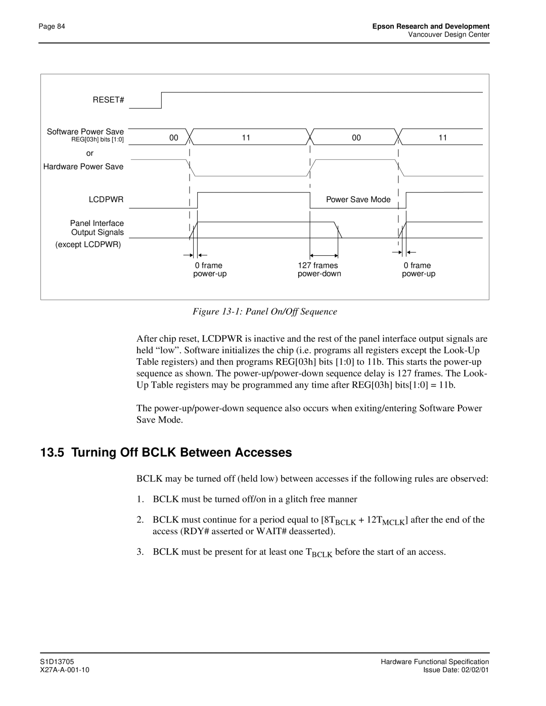
Panel Power Up/Down Sequence
Hardware Software Normal
Turning Off Bclk Between Accesses
Software Power Save
Clock Requirements
S1D13705 Internal Clock Requirements
14.0 ± 12.0 ± Index
Mechanical Data
QFP14 80 pin Unit mm
125
Sales and Technical Support
Japan North America Taiwan
This page Left Blank
Programming Notes and Examples
Document Number X27A-G-002-03
This page Left Blank
Memory Models
LCD Power Sequencing and Power Save Modes
Introduction Initialization
Look-Up Table LUT
Identifying the S1D13705 Hardware Abstraction Layer HAL
Sample Code
S1D13705 Initialization Sequence
This page Left Blank
Introduction
Initialization
Display Buffer Location
Register Values
Frame Rate Calculation
S1D13705 Initialization Sequence
Register Value hex See Also
= Horizontal Display Period in pixels
Where Pclk = Pixel clock in Hz
For a dual passive panel the formula is
= Horizontal Non-Display Period in pixels
Epson Research and Development
Memory Models
1 Bit-Per-Pixel 2 Colors/Gray Shades
Bit Pixel
2 Bit-Per-Pixel 4 Colors/Gray Shades
4 Bit-Per-Pixel 16 Colors/Gray Shades
Pixel Bit
Eight Bit-Per-Pixel 256 Colors
Green bit
Look-Up Table LUT
Look-Up Table Registers
LUT Data
Index Red Green Blue
Look-Up Table Organization
Color Modes
Unused entries
Example LUT Values for 2 Bpp Color Mode
Indicates unused entries
Bpp color
Index
Index
Gray Shade Modes
Recommended LUT Values for 1 Bpp Gray Shade
Address Red Green Blue
Suggested Values for 2 Bpp Gray Shade
Suggested LUT Values for 4 Bpp Gray Shade
Advanced Techniques
Virtual Display
REG11h Memory Address Offset Register
Registers
Examples
Offset
Panning and Scrolling
REG0Dh Screen 1 Display Start Address 1 MSB
Number of Pixels Panned Using Start Address
REG0Ch Screen 1 Display Start Address 0 LSB
REG10h Screen 1 Display Start Address 2 MSB
Panning to the left
To scroll down
Split Screen
320x240 Single Panel For Split Screen
REG12 Screen 1 Vertical Size LSB
REG13 Screen 1 Vertical Size MSB
REG0Eh Screen 2 Display Start Address 0 LSB
REG0Fh Screen 2 Display Start Address 1 MSB
Examples
REG03h Mode Register
LCD Power Sequencing and Power Save Modes
LCD Power Sequencing
Hardware Software Power Save Override Enable Bit
LCD Enable/Disable
Default Portrait Mode
Hardware Rotation
Introduction To Hardware Rotation
Portrait
Alternate Portrait Mode
REG0Dh Screen 1 Start Word Address MSB
REG1Bh Portrait Mode Register
REG0Ch Screen 1 Start Word Address LSB
REG0Eh Screen 1 Start Word Address MSB
Epson Research and Development
Power of 2. In most cases, a virtual
Default and Alternate Portrait Mode Comparison
Default Portrait Mode Alternate Portrait Mode
Limitations
Examples
Vancouver Design Center
16 , 000 FrameRate
Vancouver Design Center
Identifying the S1D13705
Contents of the Halstruct
Hardware Abstraction Layer HAL
Introduction
Using the HAL library
API for 13705HAL
Function Description
Register / Memory Access
Initialization
Int seRegisterDeviceconst Lphalstruc lpHalInfo
SeSetInit
General HAL Support
Int seGetIdint * pId
Int seSetBitsPerPixelint BitsPerPixel
Int seGetBitsPerPixelint * pBitsPerPixel
Int seGetBytesPerScanlineint * pBytes
Int seDelayint MilliSeconds
Int seGetScreenSizeint * Width, int * Height
Int seGetLastUsableBytelong * plLastByte
Int seSetPortraitMethod int Style
Advanced HAL Functions
Int seSetHighPerformanceBOOL OnOff
Int seSetHWRotateint Rotate
Int seSplitInitWORD Scrn1Addr, Word Scrn2Addr
Int seSplitScreenint Screen, int VisibleScanlines
Int seVirtInitDWORD VirtX, Dword * VirtY
Int seVirtMoveint Screen, int x, int y
SeVirtInit must be been called before calling seVirtMove
Int seSetRegint Index, Byte Value
Register / Memory Access
Int seGetRegint Index, Byte * pValue
Int seReadDisplayByteDWORD Offset, Byte *pByte
Int seReadDisplayDwordDWORD Offset, Dword *pDword
Int seWriteDisplayBytesDWORD Offset, Byte Value, Dword Count
Int seSetPowerSaveModeint PwrSaveMode
Int seGetPixellong x, long y, Dword *pColor
Drawing
Int seSetPixellong x, long y, Dword Color
Int seDrawLineint x1, int y1, int x2, int y2, Dword Color
LUT Manipulation
Int seSetLutBYTE *pLut, int Count
Int seGetLutBYTE *pLUT, int Count
Int seSetLutEntryint Index, Byte *pEntry
Int seGetLutEntryint index, Byte *pEntry
Porting Libse to a new target platform
Building the Libse library for SH3 target example
Building the HAL library for the target example
Sample code using the S1D13705 HAL API
Sample Code
Epson Research and Development
Sample code without using the S1D13705 HAL API
Purple
Pbyte
Vancouver Design Center
Pclk
Vancouver Design Center
Epson Research and Development
Vancouver Design Center
NULL, OPENEXISTING,FILEATTRIBUTENORMAL, Null
Vancouver Design Center
Header Files
Bool
Sizeversion
Errfailed
Function PROTO-TYPES
HAL EXE
Vancouver Design Center
Epson Research and Development
This page Left Blank
X27A-R-001-03
S1D13705 Register Summary X27A-R-001-03 01/02/13
13705CFG Configuration Program
Document Number X27A-B-001-03
This page Left Blank
13705CFG
This page Left Blank
13705CFG
S1D13705 Supported Evaluation Platforms
Installation
Usage
13705CFG Configuration Tabs
General Tab
Ation platform are examples of possible implementa
Decode Addresses
Values for the Register address and Display
If your hardware implementation differs from
Power
Preferences Tab
Display which requires more memory but uses less
Specification, document number X27A-A-001-xx
Clocks Tab
For details see the S1D13705 Hardware Functional
Clki frequency must be selected from the drop
Actual Clki frequency used for configuration is
Source for both Pclk and Mclk
Down list or by entering the desired frequency in MHz
Panel Tab
When the panel type is TFT, Single is automatically
Ically for configuring 8-bit color STN panels
8 bit. When an active panel type is selected
These settings define the polarity of the Fpline
Refer to S1D13705 Hardware Functional Specifi
Settings contained in the file
Complete description of the Fpframe pulse settings
Panel manufacturers recommended settings. If the file
Cation, document number X27A-A-001-xx, for a
Panel Power Tab
GPIO0 is enabled. When this box is unchecked,
Hardware Power Save function is not available
Registers Tab
13705CFG Menus
Open
Save
Save As
Configure Multiple
Export
ERD on the Web
Enable Tooltips
Comments
About 13705CFG
13705SHOW Demonstration Program
Document No. X27A-B-002-02
This page Left Blank
13705SHOW
Continuously update display memory
Download the program 13705SHOW to the system
Use alternate portrait mode
PC platform at the prompt, type
Error Did not find a 13705 device
Program Messages
This page Left Blank
13705SPLT Display Utility
Document No. X27A-B-003-02
This page Left Blank
13705SPLT
Timer is used to move screen
Enables manual split screen operation
Enables automatic split screen operation
Manual mode Move Screen 2 up Move Screen 2 down
13705SPLT Example
This page Left Blank
13705VIRT Display Utility
Document No. X27A-B-004-02
This page Left Blank
13705VIRT
Force portrait display mode to be set
Defaults to virtual width = = physical width x
Force landscape display mode to be set
Enable alternate portrait mode. Selecting this
Display
13705VIRT Example
Virtual screen shows in the upper right
Virtual screen shows in the lower left
Unable to use virtual mode at xx BPP
13705PLAY Diagnostic Utility
Document No. X27A-B-005-04
This page Left Blank
13705PLAY
Reads/writes the registers
Writes data to the LUT index when data is
Download the program 13705PLAY to the system
Writes data to the register specified by the index
13705PLAY Example
Scripting
Program Messages
This page Left Blank
13705BMP Demonstration Program
Document No. X27A-B-006-03
This page Left Blank
13705BMP
At the prompt, type
13705BMP currently views only Windows BMP format images
This error message should never bee seen. Contact ERD
Error Did not find an S1D13705 device
13705PWR Power Save Utility
Document No. X27A-B-007-03
This page Left Blank
13705PWR
Sets enables hardware power save mode REG03h bit
Download the program 13705PWR to the system
Displays this usage message
Error Did not find a 13705 device
This page Left Blank
Windows CE 2.x Display Drivers
Document Number X27A-E-001-03
X27A-E-001-03
Windows CE 2.x Display Drivers
Example Driver Builds
Ddi.dll $FLATRELEASEDIR\ddis364.dll
Ddi.dll $FLATRELEASEDIR\ddivga2.dll NK SH
Ddi.dll $FLATRELEASEDIR\ddivga8.dll NK SH
With this line Ddi.dll $FLATRELEASEDIR\EPSON.dll
Vancouver Design Center
Find the section shown below, and insert the lines as marked
If CEPCDDIS1D13705
Ddi.dll $FLATRELEASEDIR\ddis364.dll NK SH
Endif
Epson Research and Development
Installation for Cepc Environment
Copy NK.BIN and HIMEM.SYS to c\ Boot the system
Configuration
Compile Switches
Mode File
Comments
This page Left Blank
Wind River WindML v2.0 Display Drivers
Document Number X27A-E-002-03
X27A-E-002-03 Issue Date 01/04/06
Wind River WindML v2.0 Display Drivers
If necessary, generate a new mode0.h configuration file
Building a WindML v2.0 Display Driver
Make CPU=PENTIUM ugl
This page Left Blank
Wind River UGL v1.2 Display Drivers
Document Number X27A-E-003-02
X27A-E-003-02 Issue Date 01/02/13
Wind River UGL v1.2 Display Drivers
Building a UGL v1.2 Display Driver
Epson Research and Development
This page Left Blank
Linux Console Driver
Document Number X27A-E-004-02
X27A-E-004-02 Issue Date 01/09/19
Linux Console Driver
Building the Console Driver for Linux Kernel
Epson Research and Development
Vancouver Design Center
To the directory /usr/src/linux/drivers/video/epson
Vancouver Design Center
Epson Research and Development
This page Left Blank
QNX Photon v2.0 Display Driver
Document Number X27A-E-005-01
This page Left Blank
QNX Photon v2.0 Display Driver
Unpack the Graphics Driver Development Kit Archive
Configure the Driver
Building the Photon v2.0 Display Driver
Build the Driver
Installing the Driver
Run the Driver
Comments
S1D13XXX 32-Bit Windows Device Driver Installation Guide
Document No. X00A-E-003-04
X00A-E-003-04 Issue Date 01/04/17
Windows NT Version
S1D13XXX 32-Bit Windows Device Driver Installation Guide
Driver Requirements
Video Controller S1D13xxx Display Type
Windows
All PCI Bus Evaluation Cards
All ISA Bus Evaluation Cards
Windows 98/ME
Windows 95 OSR2
ADD/NEW Hardware
Previous Versions of Windows
All ISA Bus Evaluation Cards
S5U13705B00C Rev .0 ISA Bus
Document Number X27A-G-005-03
S1D13705 X27A-G-005-03 Issue Date 01/02/13
Installation and Configuration
Parts List Schematic Diagrams
This page Left Blank
S1D13705B00C Schematic Diagram 1 of 4
This page Left Blank
Features
Installation and Configuration
Configuration DIP Switch Settings
Host Bus Selection
BS# Signal Selection Pulled up to Iovdd No Connection
Jumper Settings
RD/WR# Signal Selection Pulled up to Iovdd No Connection
Iovdd Selection
LCD Interface Pin Mapping
LCD Signal Connector J5 Pinout
Pins
Even
Connector
CPU/Bus Interface Connector Pinouts
CPU/BUS Connector H1 Pinout
Comments
CPU/BUS Connector H2 Pinout
Host Bus Interface Pin Mapping
DB150 D150 WE1#
Technical Description
Embedded Memory Support
Display Adapter Card Support
ISA Bus Support
Non-ISA Bus Support
Expanded Memory Manager Support
Decoding Logic
Clock Input Support
Monochrome LCD Panel Support
LCD Panel Voltage Setting
Power Save Modes
Color Passive LCD Panel Support
Adjustable LCD Panel Negative Power Supply
Adjustable LCD Panel Positive Power Supply
13 CPU/Bus Interface Header Strips
Parts List
Item # Qty/board Designation Part Value Description
Schematic Diagrams
S1D13705B00C Schematic Diagram 1
S1D13705B00C
Vancouver Epson Research
S1D13705B00C Schematic Diagram 4
This page Left Blank
Document Number X27A-G-014-02
S1D13705 X27A-G-014-02 Issue Date 2002/09/16
CPU Interface
Introduction Features Installation and Configuration
Parts List Schematics Board Layout Technical Support
LCD Interface Pin Mapping Technical Description
This page Left Blank
Configuration DIP Switch SW1 Location
This page Left Blank
Introduction
Features
Configuration DIP Switches
Configuration DIP Switch SW1 Location
Big Endian bus interface Little Endian bus interface SW1-5
SH-4
SH-3
Not Used SW1-6
Jumper Function Position No Jumper
Configuration Jumpers
Jumper Summary
PCI Bridge Fpga
Configuration Jumper JP2 Location
Configuration Jumper JP4 Location
Configuration Jumper JP6 Location
CPU Interface
CPU Interface Pin Mapping
CPU Interface Pin Mapping
CPU Bus Connector Pin Mapping
CPU Bus Connector H1 Pinout
Connector Comments Pin No
CPU Bus Connector H2 Pinout
LCD Signal Connector J5
2LCDPWR on J5 can be inverted by setting JP6 to
Dual
Direct Host Bus Interface Support
Adjustable LCD Panel Positive Power Supply Vddh
PCI Bus Support
S1D13705 Embedded Memory
Adjustable LCD Panel Negative Power Supply Vlcd
Passive/Active LCD Panel Support
Clock Options
Software
References
Documents
Document Sources
Quantity Reference Part Description
EPF6016TC144-2 Altera EPF6016TC144-2
RD-0412 Xentek RD-0412, positive power Supply
EPN001 Xentek EPN001, negative power Supply
Pin DIP socket Machined socket, 8-pin
Schematics
S1D13705B00C Schematics 1
Schematics 2
S1D13705B00C
S1D13705B00C Schematics 3
S1D13705B00C Schematics 4
S1D13705B00C Schematics 5
Board Layout
Technical Support
Epson LCD Controllers S1D13705
Windows CE 3.x Display Drivers
Document Number X27A-E-006-01
X27A-E-006-01
Windows CE 3.x Display Drivers
Example Driver Builds
If CEPCDDIS1D13X0X
Ddi.dll $FLATRELEASEDIR\ddiflat.dll NK SH
If Cepcddiflat If CEPCDDIS1D13X0X
Endif
Epson Research and Development
Installation for Cepc Environment
EnablePreferVmem
GrayPalette
Resource Management Issues
Vancouver Design Center
Simple Display Driver Configuration
Comments
Interfacing to the Toshiba Mips TMPR3912 Microprocessor
Document Number X27A-G-004-02
This page Left Blank
Using the ITE IT8368E PC Card Buffer
Direct Connection to the Toshiba TMPR3912
Software Technical Support
This page Left Blank
S1D13705 to TMPR3912 Connection Using an IT8368E
S1D13705 to TMPR3912 Direct Connection
This page Left Blank
Introduction
Interfacing to the TMPR3912
S1D13705 Generic #1 Generic #2 Pin Names
S1D13705 Host Bus Interface
Host Bus Pin Connection
AB151 A151
Generic #1 Interface Mode
Generic #2 Interface Mode
Direct Connection to the Toshiba TMPR3912
General Description
Memory Mapping and Aliasing
S1D13705 Configuration
S1D13705 Configuration for Direct Connection
Big Endian
Using the ITE IT8368E PC Card Buffer
Hardware Description
S1D13705 to TMPR3912 Connection Using an IT8368E
16M byte
IT8368E Configuration
16M byte Card 1 IO
At 128K byte intervals
16M byte Card 2 IO
S1D13705 Configuration Using the IT8368E
= configuration for connection using ITE IT8368E
32M byte Card 2 Attribute
Software
Europe Hong Kong Singapore
Toshiba Mips TMPR3912 Processor ITE IT8368E
Japan North America Taiwan, R.O.C
Integrated Technology Express, Inc
This page Left Blank
S1D13705 Power Consumption
Document Number X27A-G-006-02
S1D13705 Power Consumption X27A-G-006-02
S1D13705 Power Consumption
S1D13705 Total Power Consumption
Conditions
Summary
This page Left Blank
Document Number X27A-G-007-04
X27A-G-007-04 Issue Date 01/02/13
Introduction Interfacing to the MC68328
Interfacing to the MC68EZ328
Interfacing to the MC68VZ328
Technical Support
List of Tables
This page Left Blank
Introduction
Interfacing to the MC68328
MC68328 System Bus
Chip-Select Module
S1D13705 MC68K #1 Generic #1 Pin Names
S1D13705 Host Bus Interface
Host Bus Pin Connection
WE0# Connect to IO V DD
Generic #1 Interface Mode
3 MC68K #1 Interface Mode
Using The MC68K #1 Host Bus Interface
MC68328 To S1D13705 Interface
Hardware Description
Using The Generic #1 Host Bus Interface
Summary of Power-On/Reset Options
2 S1D13705 Hardware Configuration
3 MC68328 Chip Select Configuration
Host Bus Interface Selection
Epson Research and Development
Interfacing to the MC68EZ328
MC68EZ328 System Bus
S1D13705 Generic #1 Pin Names
Generic #1 Interface Mode
MC683EZ28 To S1D13705 Interface
3 MC68EZ328 Chip Select Configuration
= configuration for MC68EZ328 support
Epson Research and Development
Interfacing to the MC68VZ328
MC68VZ328 System Bus
S1D13705 Host Bus Interface
Generic #1 Interface Mode
3 MC68K #1 Interface Mode
MC68VZ328 To S1D13705 Interface
CSB1 CS#
= configuration for MC68VZ328 support
3 MC68VZ328 Chip Select and Pin Configuration
Software
Motorola Inc. Motorola Literature Distribution Center, 800
Motorola Dragonball Processors
Interfacing to the NEC VR4102/VR4111 Microprocessor
Document Number X27A-G-008-02
X27A-G-008-02 Issue Date 01/02/13
VR4102/VR4111 to S1D13705 Interface
Host Bus Pin Connection Generic #2 Interface Mode
Introduction Interfacing to the NEC VR4102/VR4111
Epson LCD Controllers S1D13705 NEC Electronics Inc
This page Left Blank
NEC VR4102/VR4111 Read/Write Cycles
This page Left Blank
Introduction
Interfacing to the NEC VR4102/VR4111
NEC VR4102/VR4111 System Bus
Overview
LCD Memory Access Cycles
Lcdrdy
S1D13705 Generic #2 Pin Names
Generic #2 Interface Mode
VR4102/VR4111 to S1D13705 Interface
Busclk BS# RD/WR#
S1D13705 Hardware Configuration
See Host Bus Selection table below
NEC VR4102/VR4111 Configuration
Software
References
NEC Electronics Inc
NEC Electronics Inc. U.S.A
Santa Clara California Tel 800 Fax 800
This page Left Blank
Interfacing to the PC Card Bus
Document Number X27A-G-009-02
This page Left Blank
S1D13705 Bus Interface
Memory Access Cycles
Interfacing to the PC Card Bus
PC Card to S1D13705 Interface
This page Left Blank
PC Card Read Cycle
This page Left Blank
Introduction
PC Card System Bus
Memory Access Cycles
Interfacing to the PC Card Bus
PC Card Overview
PC Card Read Cycle
S1D13705 Bus Interface
Generic #2 Interface Mode
PC Card to S1D13705 Interface
Hardware Connections
Signal Low High
Register/Memory Mapping
Software
PC Card Pcmcia Standard March
PC Card Standard
Pcmcia
Interfacing to the Motorola MPC821 Microprocessor
Document Number X27A-G-010-02
X27A-G-010-02 Issue Date 01/02/13
Host Bus Interface Modes Generic #1 Host Bus Interface Mode
Introduction Interfacing to the MPC821
MPC821 to S1D13705 Interface
This page Left Blank
List of Tables
This page Left Blank
Introduction
Interfacing to the MPC821
MPC8xx System Bus
MPC821 Bus Overview
Power PC Memory Read Cycle
Normal Non-Burst Bus Transactions
Power PC Memory Write Cycle
Burst Cycles
Memory Controller Module
General-Purpose Chip Select Module Gpcm
User-Programmable Machine UPM
Host Bus Interface Modes
Generic #1 Host Bus Interface Mode
MPC821 to S1D13705 Interface
Typical Implementation of MPC821 to S1D13705 Interface
MPC821ADS Evaluation Board Hardware Connections
List of Connections from MPC821ADS to S1D13705
P12-A3, P12-B3, P12-A4, P12-B4
P6-A14 WE0#
P12-A1, P12-B1, P12-A2, P12-B2
P12-A5, P12-B5, P12-A6, P12-B6
Configuration Settings
MPC821 Chip Select Configuration
Test Software
1FFE0
Epson Research and Development
Software
Motorola Inc. Literature Distribution Center 800
Epson LCD/CRT Controllers S1D13705
Motorola MPC821 Processor
Interfacing to the Motorola MCF5307 ColdFire Microprocessor
Document Number X27A-G-011-02
X27A-G-011-02 Issue Date 01/02/13
Host Bus Pin Connection Generic #1 Interface Mode
Introduction Interfacing to the MCF5307
Epson LCD Controllers S1D13705 Motorola MCF5307 Processor
This page Left Blank
List of Tables
This page Left Blank
Introduction
Interfacing to the MCF5307
MCF5307 System Bus
MCF5307 Memory Read Cycle
Chip-Select Module
S1D13705 Bus Interface
Generic #1 Interface Mode
MCF5307 To S1D13705 Interface
Typical Implementation of MCF5307 to S1D13705 Interface
Little Endian Big Endian = configuration for MFC5307 support
MCF5307 Chip Select Configuration
Software
References
Motorola MCF5307 Processor
Interfacing to the Philips Mips PR31500/PR31700 Processor
Document Number X27A-G-012-02
This page Left Blank
Direct Connection to the Philips PR31500/PR31700
This page Left Blank
S1D13705 to PR31500/PR31700 Connection Using an IT8368E
S1D13705 to PR31500/PR31700 Direct Connection
This page Left Blank
Introduction
Interfacing to the PR31500/PR31700
S1D13705 Host Bus Interface
Generic #1 Interface Mode
Generic #2 Interface Mode
Direct Connection to the Philips PR31500/PR31700
S1D13705 to PR31500/PR31700 Direct Connection
Memory Mapping and Aliasing
S1D13705 Configuration and Pin Mapping
Using the ITE IT8368E PC Card Buffer
S1D13705 to PR31500/PR31700 Connection Using an IT8368E
S1D13705 S1D13705 aliased 128 times 0900 0000h
S1D13705 Configuration
Software
Philips Mips PR31500/PR31700 Processor
Philips Semiconductors
S5U13704/5 TMPR3912/22U CPU Module
Document Number X00A-G-004-02
S5U13704/5 TMPR3912/22U CPU Module
Table of Contents
This page Left Blank
List of Tables
List of Figures
This page Left Blank
General Description
S1D13704/5 Bus Interface
Bus Interface Modes
Generic #2 Interface Mode
TMPR3912/22U and S1D13704/5 Interface
Hardware Connections
Memory Mapping and Aliasing
S1D13704/5 Configuration and Pin Mapping
= configuration for Toshiba TMPR3912/22U host bus interface
S1D13704/5 Generic #2 Interface Pin Mapping
CPU Module Description
Clock Signals Busclk
LCD Connectors 1 50-pin LCD Module Connector, J3
Clki
Lcdpwr Polarity
Standard Epson LCD Connector, J4
LCD Controller 1 S1D13704 vs. S1D13705
3 S1D13704\75 Chip Select
This page Left Blank
Interfacing to the NEC VR4181A Microprocessor
Document Number X27A-G-013-02
X27A-G-013-02
NEC VR4181A System Bus Overview LCD Memory Access Signals
Introduction Interfacing to the NEC VR4181A
VR4181A to S1D13705 Interface
This page Left Blank
Typical Implementation of VR4181A to S1D13705 Interface
This page Left Blank
Introduction
Interfacing to the NEC VR4181A
NEC VR4181A System Bus
LCD Memory Access Signals
BHE#
Generic #2 Interface Mode
VR4181A to S1D13705 Interface
Typical Implementation of VR4181A to S1D13705 Interface
S1D13705 Hardware Configuration
NEC VR4181A Configuration
Software
References
Technical Support
This page Left Blank
Interfacing to an 8-bit Processor
Document Number X27A-G-015-01
X27A-G-015-01 Issue Date 01/12/20
Bit Processor to S1D13705 Interface
Interfacing to an 8-bit Processor
Generic 8-bit Processor System Bus
Epson LCD/CRT Controllers S1D13705
This page Left Blank
List of Tables
This page Left Blank
Introduction
Interfacing to an 8-bit Processor
Generic 8-bit Processor System Bus
S1D13705 Generic #2 Description Pin Names
Generic #2 Interface Mode
Bit Processor to S1D13705 Interface
= required configuration for this application
Little Endian Big Endian
Software
References
Technical Support
This page Left Blank