STUDIO3511/4511
Toshiba TEC Corporation
General Precautions Regarding the Installation
Service of Machines
Main Service Parts for Safety
Contents
Control Panel
Control circuit for the exposure lamp
10.1
10-1
10.2
10-5
12.1
12-1
12.2
12.3
15.1
15-1
15.2
15.3
STUDIO3511/4511 Contents November 2003 Toshiba TEC
SPECIFICATIONS/ACCESSORIES/OPTIONS/SUPPLIES
Specifications
System copy speed
ADU PFP LCF
Automatic duplexing unit Stackless/switchback type
To 550 sheets 64-80 g/m2 17-22 lb. Bond
Sheets 64-80 g/m2 17-22 lb. Bond
M2 17-22 lb. Bond
718
Accessories
Options
Supplies
System List
STAPLE-2000
Radf
STAPLE-600
STUDIO3511/4511 Specifications November 2003 Toshiba TEC
Sectional View
Outline of the Machine
Front side view
Recovery blade
Drum cleaning blade
Drum cleaner brush
Toner recovery auger
Rear side view Drive system
Drum cleaner brush motor
Scan motor
Main motor
Transport motor
Unit construction
Electric Parts Layout
Front side
Scanner unit Motor, sensor, lamp
A4 series
LT series
EXP
Switch, PC board, heater, thermostat, other part
DH1
ASD/AUD/CND/SAD/TWD models Standard NAD/MJD models Option
Control panel unit
Process unit Motor, sensor, switch, clutch, solenoid
S25 S26 M13 Front side
Motor, switch
Laser unit
Paper feeder unit
Transport unit
CLT3
CLT5
Bypass unit
Automatic duplexing unit
SFB CLT6 SOL3
ADU CLT7
Fuser unit
Drive unit
LGC SYS
PC board unit
HDD NIC BRK
Symbols and Functions of Various Components
Sensors and switches
CCL-F-POS-SW
CCL-R-POS-SW
CST-U-TRY-SNR
CST-L-TRY-SNR
Electromagnetic clutches
Solenoids
PC boards
Lamps and heaters
Thermistors and thermostats
Transformer
Others
24GeneralDescription
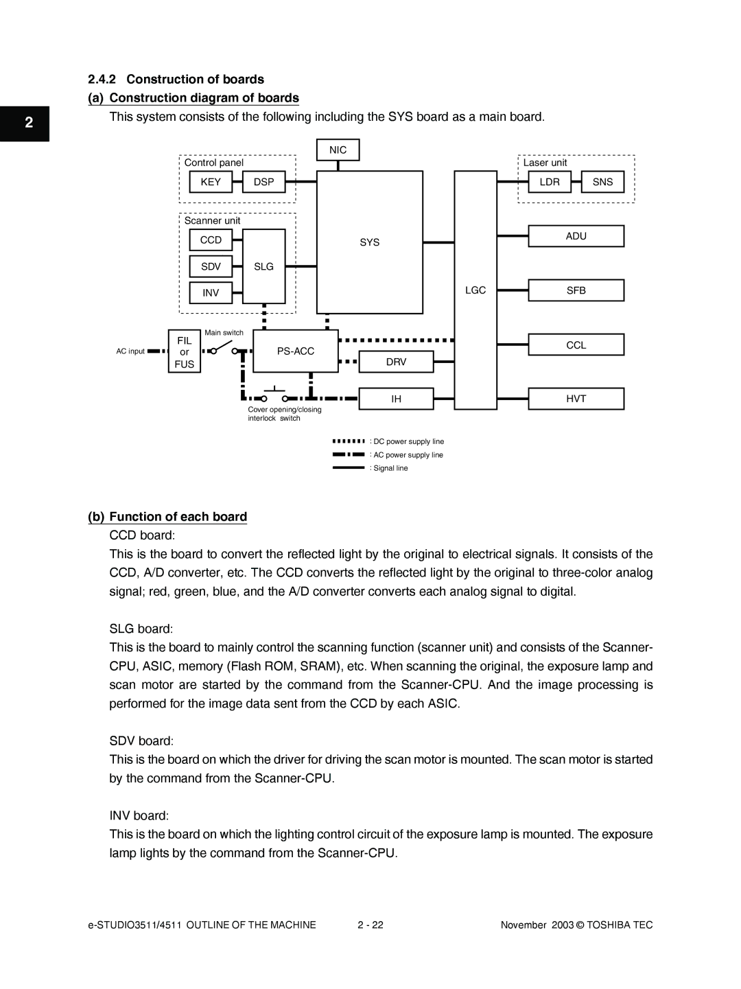
Construction of boards Construction diagram of boards
Function of each board CCD board
Page
HVT
Covers Front cover / Toner bag
Disassembly and Replacement of Covers and PC boards
Receiving tray
Tray back cover
Front lower cover
Front right cover
Left cover
Left rear cover
Left upper cover
Front upper cover
Right upper cover
IH terminal cover
Right rear cover
Right lower cover
Right rear hinge cover
Right front hinge cover
Rear cover
Upper rear cover
LGC board
PC boards Logic PC board LGC board A-1 LGC board case
Hard disk HDD
System control PC board case SYS board case
Remove 4 screws and take off the SYS board case
NIC board / System control PC board SYS board
High-voltage transformer
Power supply unit
Flow
Noise filter
Fuse board FUS board
Driving PC board DRV board
Options MR-3015 Reversing Automatic Document Feeder Radf
Page
Heater is installed
KD-1011 Paper Feed Pedestal PFP
KD-1012 Large Capacity Feeder LCF
Page
MJ-1022 Hanging finisher When PFP/LCF is not installed
Lift up the equipment and take off the LCF
When PFP/LCF is installed
Remove 2 screws Lift up the finisher and take it off
Page
MJ-1023 Console finisher
MJ-1024 Console finisher
Page
MJ-6004 Hole punch unit
Page
Remove 2 screws Lift up the punch unit and take it off
KN-3511 Bridge unit
November 2003 Toshiba TEC
Copy Process
Expression of Colors and 4-Step Copy Process
General Description of Copying Process
Photocon
Details of Copying Process
CCD board
White background Image is not Developed
Photoconductive
Photoconductive Layer Aluminum Base
Blade cleaning
Recovery blade Drum rotation
List of Copying Process Conditions
Pressure roller Silicon sponge
STUDIO3511/4511 Copy Process November 2003 Toshiba TEC
General Operation
Overview of Operation
Description of Operation
Warming-up
Ready ready for copying
Drawer feed copying Upper drawer paper feeding
Page
Page
Scan motor fwd
Bypass feed copying
Interruption copying
Types of abnormality
Detection of Abnormality
Description of abnormality A-1 Add paper
STUDIO3511/4511 General Operation November 2003 Toshiba TEC
Approx 1.2 seconds
Registration clutch turned on ↓ Approx 1.2 sec
Paper jam E010 → The copying operation is Stopped
Exit sensor detects jamming of the trailing edge Paper
Registration clutch turned OFF
After approx 1.3 seconds
Paper jam E020 → The copying operation is
November 2003 Toshiba TEC STUDIO3511/4511 General Operation
Flow Chart
Power on to ready
Ready
Automatic feed copying
Main charger on
YES
Control Panel
Control Panel and Display Panel
Items Shown on the Display Panel
Display
Saddle Stitch
Tray Full Ready
Change Drawer To Correct Paper Size
Copying
Large Capacity Feeder Cannot Punch
Check Paper
This Size Paper
Department
Counter
To Correct Media Type Press Basic
Radf
Dot matrix LCD circuit
Structure
Frame
Data Transmission
Load Frame
LED display circuit
Method of LED display ex Displaying Copy
Stopper
Disassembly and Replacement
Slide the stopper and pull it out
November 2003 Toshiba TEC STUDIO3511/4511 Control Panel
Remove 16 screws and take off the KEY board
Scanner
Function
Construction
Mirror-2 Mirror-3
Scan motor
Scanning drive circuit
PS-ACC-350
Input/output signals
Initialization at power-ON
Onno YES
OFF YES
On no YES
Control of Exposure Lamp
General description
PWA-CCD CCD PWA-CCDPWA-SLG
CPU
Exposure lamp
Control circuit for the exposure lamp
Opto-electronic conversion
General Description of CCD Control
Shading correction
Principle of original size detection
Automatic Original Size Detection Circuit
Process of detection of original size
APS-3
APS-1 APS-2
APS-C APS-R APS-2 APS-3
APS-C APS-R APS-1 APS-2 APS-3
ST-R
Original LEDPhototransistor
Lens cover
Original glass
SLG board cooling fan
Automatic original detection sensor APS sensor A4 series
LT series
Lens unit
Carriages-1
Carriage-1
Carriage Refer to the Service Handbook for more details
Carriage home position sensor
Platen sensor
Scanning section control PC board SLG board
General Description
Image Processing
Followings are the boards used for image processing
CCD
Configuration
-201 shows the image processing section of this equipment
Asic
Asic ACS
Features
SYS Board PWA-F-SYS-350
Functions of image processing circuit
Example
’ = + b +
Example Enlargement
Example Reduction
Paper
November 2003 Toshiba TEC STUDIO3511/4511 Image Processing
LGC Board PWA-F-LGC-350
Laser Driving PC Board LDR Board
Laser Optical Unit
Writing Section Overview
Structure
STUDIO3511/4511 Laser Optical Unit November 2003 Toshiba TEC
Deviation
STUDIO3511/4511 Laser Optical Unit November 2003 Toshiba TEC
Laser power comparison circuit Laser driver Circuit Constant
Polygonal motor ON/OFF signal
Polygonal motor reference clock signal
Laser Unit Cooling Fan
Polygonal Motor
Laser optical unit
Laser unit cooling fan
Drive System
Main Motor
Construction
Signal level of motor circuit
Drive circuit of main motor
Transport Motor
Drive circuit of transport motor
Developer Motor
Developer motor on signal
Developer motor rotational direction signal
Developer motor reference clock signal
Normal Out of control Developer motor PLL signal
Developer motor drive unit
Remove 2 screws and take off the developer motor
Developer motor
Black developer lifting clutch
Transport motor drive unit
Setscrew
Transport motor drive unit Connector
Main motor drive unit
Tension plate
Motor
STUDIO3511/4511 Drive System November 2003 Toshiba TEC
Paper Feeding System
General Descriptions
Page
Paper Feeding Section Sectional View Front side
Paper Feeding Section Drive System Rear side
Operation of bypass pickup roller
Operation of drawer pickup roller
Separation of paper
Ready status
General operation From power-ON to ready status
Bypass feeding
Drawer feedingD-1 Lower drawer
IN1 IN2 Brake CCW
Drive Circuit of Tray-up Motor
Stop
Bypass unit A-1 Bypass unit
Bypass tray slide guide width detection PC board
Bypass transport roller
Bypass pickup roller
Bypass pickup solenoid
Bypass paper sensor
Bypass feed roller
Bypass separation roller
Remove the arbor, shaft and spring
Lower drawer feed sensor/Side cover opening/closing switch
Bypass feed sensor
Upper drawer feed sensor/Registration sensor
Registration roller
Drawer feeding unit E-1 Drawer feeding unit
Feed clutch
Separation roller
Remove 1 screw and take off the separation roller holder
Pickup roller
CLUTCH-6-L
Remove the pulley, one-way clutch and 3 E-rings
Feed roller
6Drawer tray-up sensor and Drawer empty sensor
Drawer paper stock sensor
Tray drive unit
Tray drive unit
Lower transport clutch Low/High speed
Registration guide
Middle guide
Drum Related Section
Functions
Page
Output Control Circuits of High-Voltage Transformer
IC7
Drum Temperature Detection Circuit
CPU
Temperature/Humidity Sensor
Charger Wire Cleaner
Operation
Drive circuit
Cleaner unit
Cleaner unit
Main charger unit B-1 Main charger unit
Main charger grid
Wire pad
Charger wire
Remove 1 screw and take off the pad guide
Remove the base
Drum
Recovery blade
Cleaner Drum cleaning blade
Drum cleaner brush
Discharge LED unit F-1 Discharge LED
Drum thermistor
Remove the discharge LED
Charger cleaner motor
Charger cleaner detection switch
Toner bag full detection sensor-2
Ozone filter
Temperature/Humidity sensor
Ozone exhaust fan
Latch
Page
Developer Unit
Color auto-toner sensor Mixer Developer sleeve
General descriptions
Black Toner Cartridge Drive Unit
Toner motor
Black Developer Unit
Functions
Black developer unit drive section
LCA301-1
Black auto-toner sensor circuit
Converter
Magnetic circuit
STUDIO3511/4511 Developer Unit November 2003 Toshiba TEC
Black developer unit lifting mechanism
Color Developer Unit
Color developer unit drive section
Gear G21
Color auto-toner sensor circuit
Page
Color toner supply
High-Voltage Transformer Output Control Circuit
CDVDON-0 CDVAON-0
Black developer unit A-1 Black developer unit
Developer material
Auto-toner sensor
Pour the developer material
Doctor blade
Remove 2 screws and take off the doctor blade
Developer sleeve
Mixer
Take off the mixer from the hole of front side
Color developer unit B-1 Developer material
Discharge the developer material Pour the developer material
Gear assembly
Procedure for replacing an oil seal
Black developer lifting unit
Take off the black developer toner supply unit .7 K
Remove 2 screws and take off the cleaner rail stay
Black toner supply unit
Cartridge switch with the whole bracket
Remove 2 screws and take off the toner motor
Black toner supply auger unit
STUDIO3511/4511 Developer Unit November 2003 Toshiba TEC
Revolver Unit
STUDIO3511/4511 Revolver Unit November 2003 Toshiba TEC
Drive of Revolver Unit
Revolver Motor Drive Circuit
Revolver motor
Operation
Home position detection
Escape position movement
During warming-up
During image quality control
Color toner cartridge
Color developer unit
Color toner cartridge sensor
Rear Front
Remove 1 screw and take off the color toner cartridge sensor
Revolver home position sensor
Revolver unit
Lock lever
Remove 5 screws and take off the bracket
Internal cooling fan
Transfer Unit
STUDIO3511/4511 Transfer Unit November 2003 Toshiba TEC
Page
Outline of 1st transfer
Outline of 2nd transfer
High-Voltage Power Supply
LCA-301-1
1000V
PWA
Transfer belt unit
Loosen 3 screws and take off the bracket
Transfer belt
Stand plate short
1st transfer roller
Transfer belt home position sensor-1
Transfer belt home position sensor-2
Transfer belt cleaning unit
Remove 1 screw and take off the bracket on the front side
Conductive tape
Harness clamp Transfer belt cleaner auger motor
2nd transfer roller
2nd transfer unit
2nd transfer roller contact clutch
2nd transfer roller position detection sensor
Paper clinging detection sensor
Paper clinging detection sensor Bracket
Page
Image Quality Control
Principle of the Sensor
Flow Chart of Control Procedure
YES
Various image forming conditions
Image quality sensor / Image quality sensor Shutter solenoid
Fuser Unit / Paper Exit Section
Functions
Page
Configuration
Heater Control Circuit
Heating principle of IH Heater
Book Diagram of High Frequency Power Supply
Image of Current Flowing form a to B
IH control circuit interface
+5VSW
IH2 on
IH1 on
OFF
For ASD, AUD, CND
FAX
Temperature detection section
Control of the surface temperature of the fuser belt
Energy Saver
Reference
PC4/AN4
Condtion Priority of error checking
Abnormality in the IH control circuit
IH error
Control Circuit of Exit Motor
Exit Motor Drive
Oil roller
Cleaning roller
Rear side
IH coil
Fuser roller / Fuser belt guide
Bearing Fuser belt guide
Fuser belt
Separation finger
Separation finger unit
Pressure roller
Thermostat
Remove 2 screws and take off the thermostat from the bracket
Thermistor
Exit sensor / Exit finger / Transport guide
Exit roller
IH control PC board IH board
IH control board cooling fan
Flow
Scraper
Automatic Duplexing Unit ADU
Description of Operations
Page
Page
Page
Equipment
Unit msec
Exit sensor Registration sensor Registration clutch
ADU entrance sensor ADU exit sensor ADU clutch ADU motor
Drive of ADU
Yes
Command signal
Power Supply Unit
Operation of DC Output Circuits
Output Channel
November 2003 Toshiba TEC STUDIO3511/4511 Power Supply Unit
Charger cleaner motor Power supply Power supply cooling fan
Fuse
Bridge unit +24VD2
F54A Semi time-lag +24VD4
Configuration of Power Supply Unit
Toshiba
PWR-DN
Sequence of Power Supply
PWR-EN
AC Wire Harness
Scanner
STUDIO3511/4511 Power Supply Unit November 2003 Toshiba TEC
PC Boards
PWA-F-LGC
PWA-F-SLG PWA-F-CCD PWA-F-SDV
PWA-F-DRV
PWA-F-LDR PWA-F-SNS
PWA-F-ADU
PWA-F-DSP PWA-F-KEY
NAD/SAD/TWD models Standard
PWA-F-FIL
PWA-F-FUS ASD/AUD/CND models Standard, MJD model Option
STUDIO3511/4511 PC Boards November 2003 Toshiba TEC
Page
Kanda NISHIKI-CHO, CHIYODA-KU, TOKYO, 101-8442 Japan