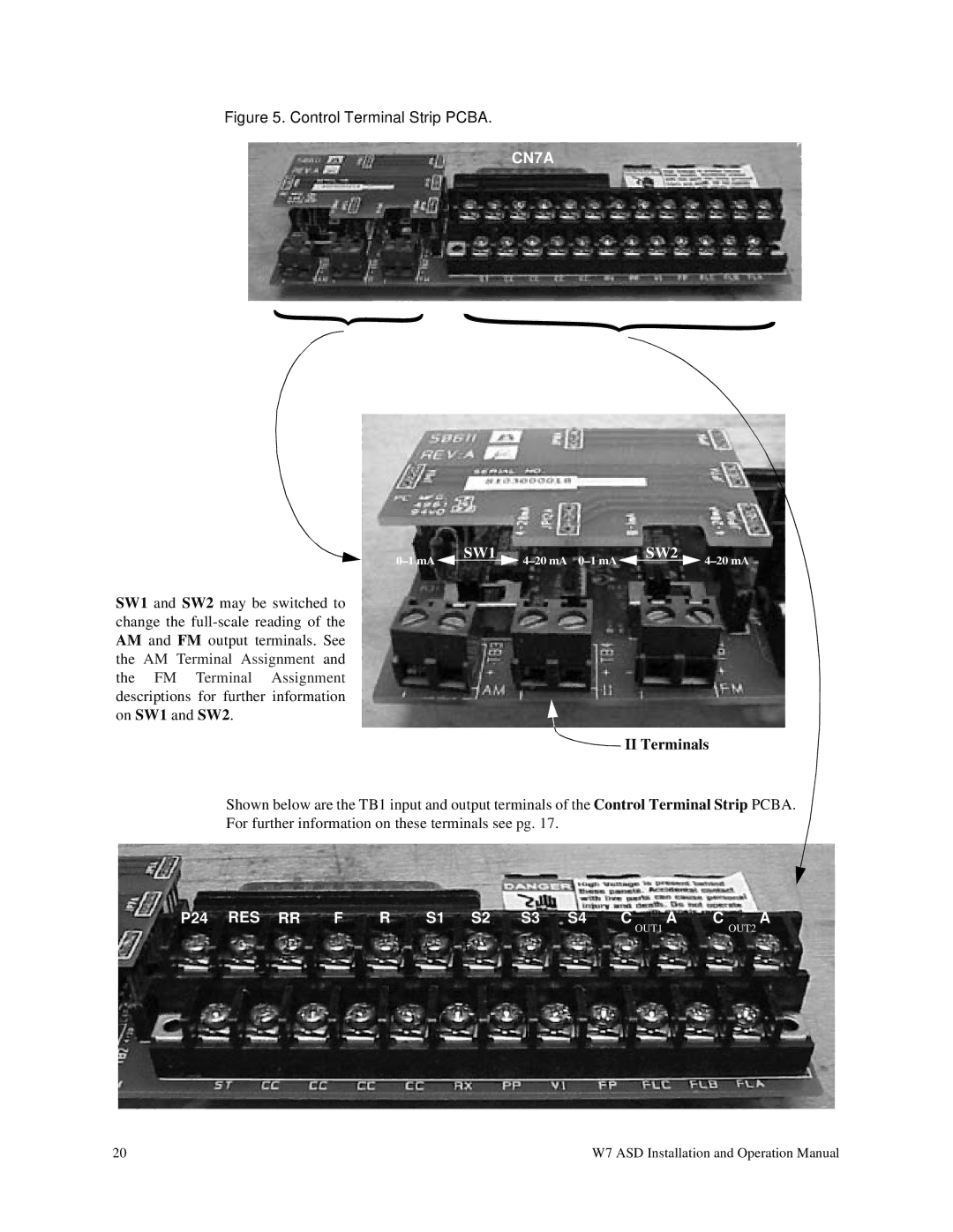
Figure 5. Control Terminal Strip PCBA.
CN7A | 1 |
|
{
{
SW1 | SW2 | |||
|
|
SW1 and SW2 may be switched to change the
 II Terminals
Shown below are the TB1 input and output terminals of the Control Terminal Strip PCBA. For further information on these terminals see pg. 17.
P24 RES RR | F | R | S1 S2 S3 S4 | C | A | C | A |
|
|
|
|
| OUT1 |
| OUT2 |
20 | W7 ASD Installation and Operation Manual |