Inverter PCB

The inverter PCB provides the current and voltage phase the scanning lamp requires.

Scanning lamp

The scanning lamp illuminates the source document, which causes reflected light from the glass to be directed to the CCD driver PCB for document imaging.
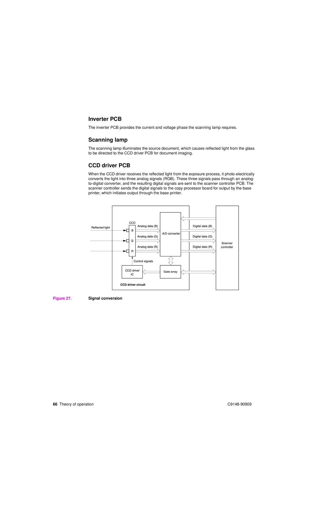
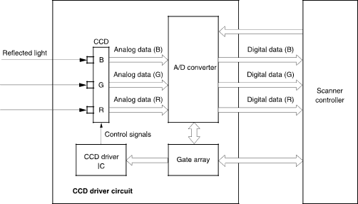
CCD driver PCB

When the CCD driver receives the reflected light from the exposure process, it photo-electrically converts the light into three analog signals (RGB). These three signals pass through an analog- to-digital converter, and the resulting digital signals are sent to the scanner controller PCB. The scanner controller sends the digital signals to the copy processor board for output by the base printer, which initiates output through the base printer.


Figure 27.

Signal conversion


66 Theory of operation

C9148-90909