Signal Description
R
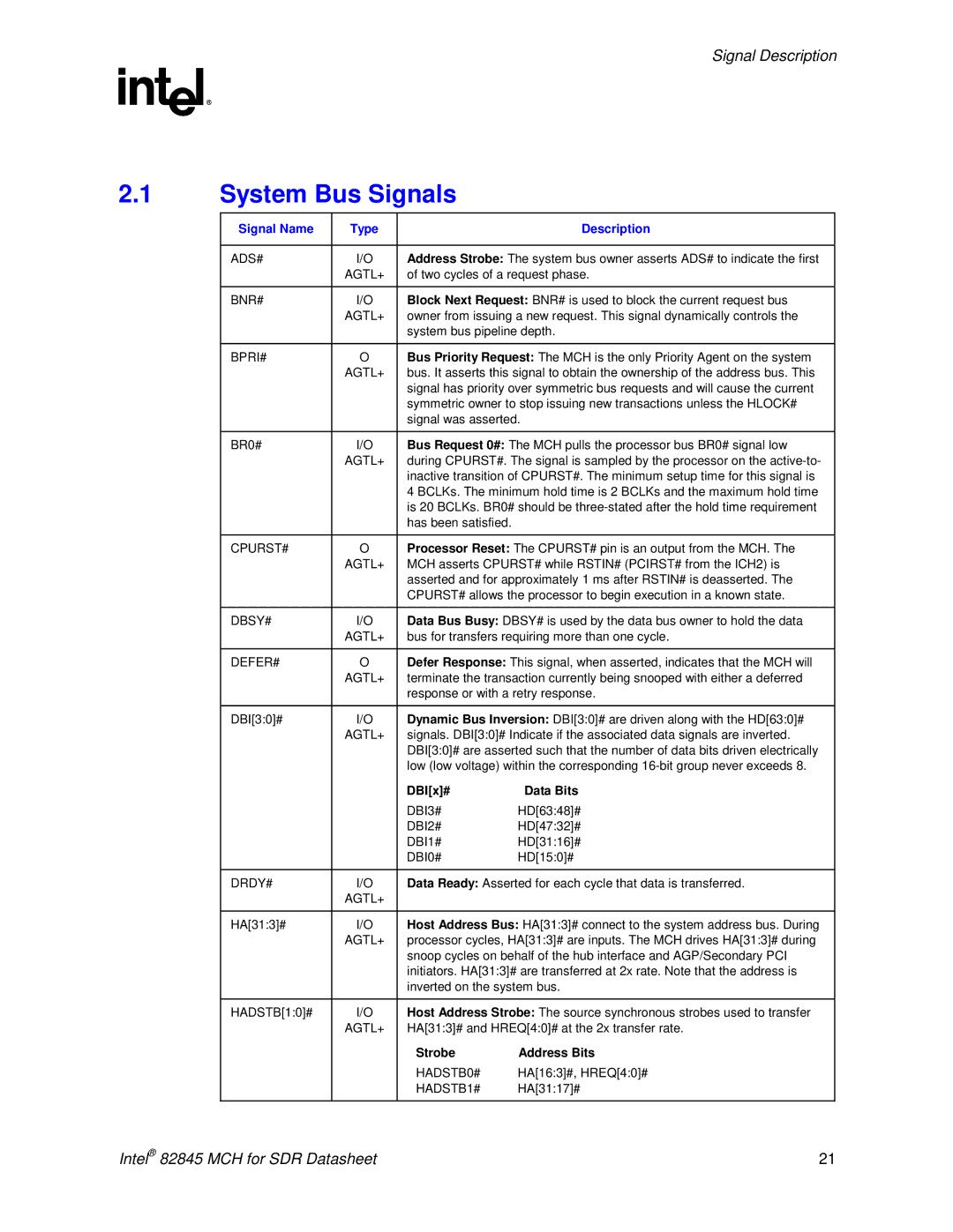
2.1System Bus Signals
Signal Name | Type |
| Description |
|
|
| |
ADS# | I/O | Address Strobe: The system bus owner asserts ADS# to indicate the first | |
| AGTL+ | of two cycles of a request phase. | |
|
|
| |
BNR# | I/O | Block Next Request: BNR# is used to block the current request bus | |
| AGTL+ | owner from issuing a new request. This signal dynamically controls the | |
|
| system bus pipeline depth. | |
|
|
| |
BPRI# | O | Bus Priority Request: The MCH is the only Priority Agent on the system | |
| AGTL+ | bus. It asserts this signal to obtain the ownership of the address bus. This | |
|
| signal has priority over symmetric bus requests and will cause the current | |
|
| symmetric owner to stop issuing new transactions unless the HLOCK# | |
|
| signal was asserted. | |
|
|
| |
BR0# | I/O | Bus Request 0#: The MCH pulls the processor bus BR0# signal low | |
| AGTL+ | during CPURST#. The signal is sampled by the processor on the | |
|
| inactive transition of CPURST#. The minimum setup time for this signal is | |
|
| 4 BCLKs. The minimum hold time is 2 BCLKs and the maximum hold time | |
|
| is 20 BCLKs. BR0# should be | |
|
| has been satisfied. |
|
|
|
| |
CPURST# | O | Processor Reset: The CPURST# pin is an output from the MCH. The | |
| AGTL+ | MCH asserts CPURST# while RSTIN# (PCIRST# from the ICH2) is | |
|
| asserted and for approximately 1 ms after RSTIN# is deasserted. The | |
|
| CPURST# allows the processor to begin execution in a known state. | |
|
|
| |
DBSY# | I/O | Data Bus Busy: DBSY# is used by the data bus owner to hold the data | |
| AGTL+ | bus for transfers requiring more than one cycle. | |
|
|
| |
DEFER# | O | Defer Response: This signal, when asserted, indicates that the MCH will | |
| AGTL+ | terminate the transaction currently being snooped with either a deferred | |
|
| response or with a retry response. | |
|
|
| |
DBI[3:0]# | I/O | Dynamic Bus Inversion: DBI[3:0]# are driven along with the HD[63:0]# | |
| AGTL+ | signals. DBI[3:0]# Indicate if the associated data signals are inverted. | |
|
| DBI[3:0]# are asserted such that the number of data bits driven electrically | |
|
| low (low voltage) within the corresponding | |
|
| DBI[x]# | Data Bits |
|
| DBI3# | HD[63:48]# |
|
| DBI2# | HD[47:32]# |
|
| DBI1# | HD[31:16]# |
|
| DBI0# | HD[15:0]# |
|
|
| |
DRDY# | I/O | Data Ready: Asserted for each cycle that data is transferred. | |
| AGTL+ |
|
|
|
|
| |
HA[31:3]# | I/O | Host Address Bus: HA[31:3]# connect to the system address bus. During | |
| AGTL+ | processor cycles, HA[31:3]# are inputs. The MCH drives HA[31:3]# during | |
|
| snoop cycles on behalf of the hub interface and AGP/Secondary PCI | |
|
| initiators. HA[31:3]# are transferred at 2x rate. Note that the address is | |
|
| inverted on the system bus. | |
|
|
| |
HADSTB[1:0]# | I/O | Host Address Strobe: The source synchronous strobes used to transfer | |
| AGTL+ | HA[31:3]# and HREQ[4:0]# at the 2x transfer rate. | |
|
| Strobe | Address Bits |
|
| HADSTB0# | HA[16:3]#, HREQ[4:0]# |
|
| HADSTB1# | HA[31:17]# |
|
|
|
|
Intel® 82845 MCH for SDR Datasheet | 21 |