Register Description
R
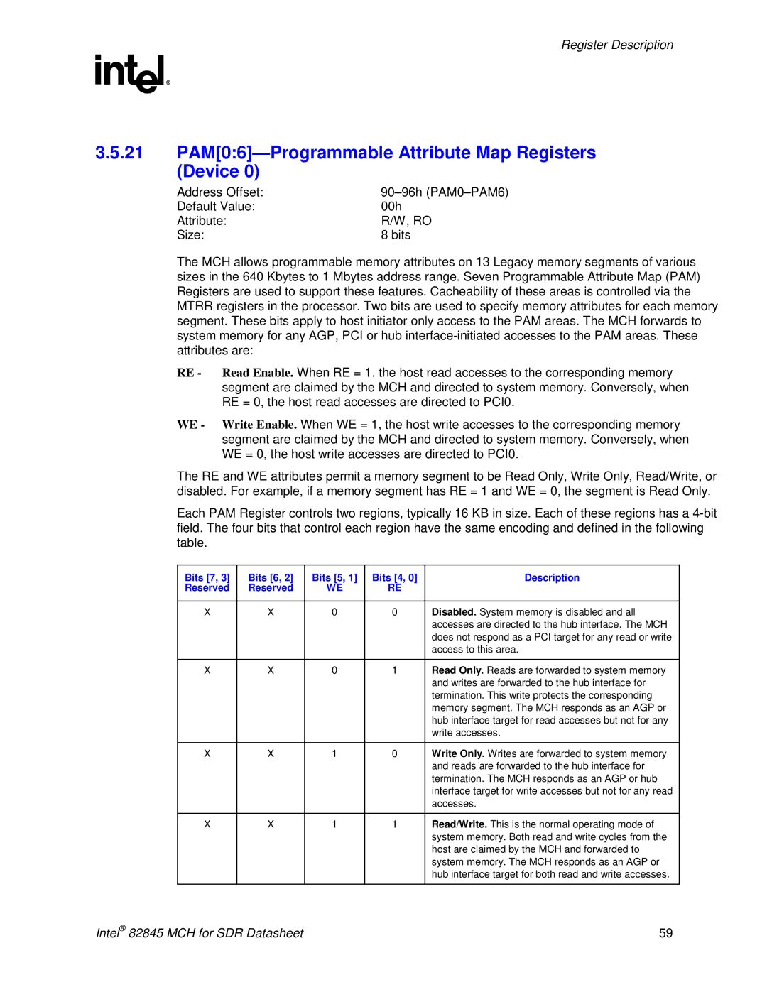
3.5.21PAM[0:6]—Programmable Attribute Map Registers (Device 0)
Address Offset: | |
Default Value: | 00h |
Attribute: | R/W, RO |
Size: | 8 bits |
The MCH allows programmable memory attributes on 13 Legacy memory segments of various sizes in the 640 Kbytes to 1 Mbytes address range. Seven Programmable Attribute Map (PAM) Registers are used to support these features. Cacheability of these areas is controlled via the MTRR registers in the processor. Two bits are used to specify memory attributes for each memory segment. These bits apply to host initiator only access to the PAM areas. The MCH forwards to system memory for any AGP, PCI or hub
RE - Read Enable. When RE = 1, the host read accesses to the corresponding memory segment are claimed by the MCH and directed to system memory. Conversely, when RE = 0, the host read accesses are directed to PCI0.
WE - Write Enable. When WE = 1, the host write accesses to the corresponding memory segment are claimed by the MCH and directed to system memory. Conversely, when WE = 0, the host write accesses are directed to PCI0.
The RE and WE attributes permit a memory segment to be Read Only, Write Only, Read/Write, or disabled. For example, if a memory segment has RE = 1 and WE = 0, the segment is Read Only.
Each PAM Register controls two regions, typically 16 KB in size. Each of these regions has a
Bits [7, 3] | Bits [6, 2] | Bits [5, 1] | Bits [4, 0] | Description |
Reserved | Reserved | WE | RE |
|
|
|
|
|
|
X | X | 0 | 0 | Disabled. System memory is disabled and all |
|
|
|
| accesses are directed to the hub interface. The MCH |
|
|
|
| does not respond as a PCI target for any read or write |
|
|
|
| access to this area. |
|
|
|
|
|
X | X | 0 | 1 | Read Only. Reads are forwarded to system memory |
|
|
|
| and writes are forwarded to the hub interface for |
|
|
|
| termination. This write protects the corresponding |
|
|
|
| memory segment. The MCH responds as an AGP or |
|
|
|
| hub interface target for read accesses but not for any |
|
|
|
| write accesses. |
|
|
|
|
|
X | X | 1 | 0 | Write Only. Writes are forwarded to system memory |
|
|
|
| and reads are forwarded to the hub interface for |
|
|
|
| termination. The MCH responds as an AGP or hub |
|
|
|
| interface target for write accesses but not for any read |
|
|
|
| accesses. |
|
|
|
|
|
X | X | 1 | 1 | Read/Write. This is the normal operating mode of |
|
|
|
| system memory. Both read and write cycles from the |
|
|
|
| host are claimed by the MCH and forwarded to |
|
|
|
| system memory. The MCH responds as an AGP or |
|
|
|
| hub interface target for both read and write accesses. |
|
|
|
|
|
Intel® 82845 MCH for SDR Datasheet | 59 |