Register Description
R
3.5.27AGPCMD—AGP Command Register (Device 0)
Address Offset: | |
Default Value: | 0000_0000h |
Access: | R/W |
Size: | 32 bits |
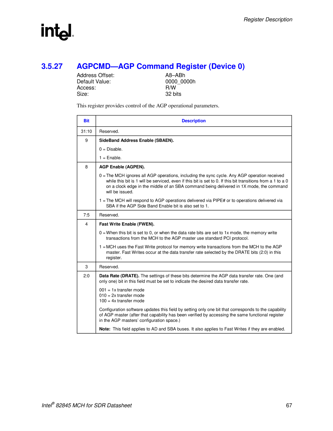
This register provides control of the AGP operational parameters.
Bit |
| Description |
|
| |
31:10 | Reserved. | |
|
| |
9 | SideBand Address Enable (SBAEN). | |
| 0 | = Disable. |
| 1 | = Enable. |
|
| |
8 | AGP Enable (AGPEN). | |
| 0 | = The MCH ignores all AGP operations, including the sync cycle. Any AGP operation received |
|
| while this bit is 1 will be serviced, even if this bit is set to 0. If this bit transitions from a 1 to a 0 |
|
| on a clock edge in the middle of an SBA command being delivered in 1X mode, the command |
|
| will be issued. |
| 1 | = The MCH will respond to AGP operations delivered via PIPE# or to operations delivered via |
|
| SBA if the AGP Side Band Enable bit is also set to 1. |
|
| |
7:5 | Reserved. | |
|
| |
4 | Fast Write Enable (FWEN). | |
| 0 | = When this bit is set to 0, or when the data rate bits are set to 1x mode, the memory write |
|
| transactions from the MCH to the AGP master use standard PCI protocol. |
| 1 | = MCH uses the Fast Write protocol for memory write transactions from the MCH to the AGP |
|
| master. Fast Writes occur at the data transfer rate selected by the DRATE bits (2:0) in this |
|
| register. |
|
| |
3 | Reserved. | |
|
| |
2:0 | Data Rate (DRATE). The settings of these bits determine the AGP data transfer rate. One (and | |
| only one) bit in this field must be set to indicate the desired data transfer rate. | |
| 001 = 1x transfer mode | |
| 010 = 2x transfer mode | |
| 100 = 4x transfer mode | |
| Configuration software updates this field by setting only one bit that corresponds to the capability | |
| of AGP master (after that capability has been verified by accessing the same functional register | |
| in the AGP masters’ configuration space.) | |
| Note: This field applies to AD and SBA buses. It also applies to Fast Writes if they are enabled. | |
|
|
|
Intel® 82845 MCH for SDR Datasheet | 67 |
