Register Description
R
Bit |
| Description |
|
| |
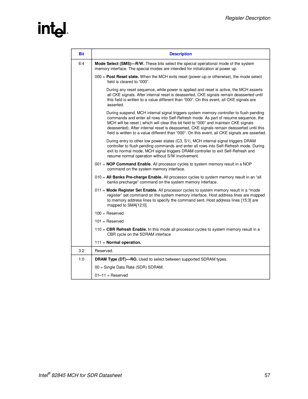
6:4 | Mode Select | |
| memory interface. The special modes are intended for initialization at power up. | |
| 000 | = Post Reset state. When the MCH exits reset |
|
| field is cleared to “000”. |
|
| During any reset sequence, while power is applied and reset is active, the MCH asserts |
|
| all CKE signals. After internal reset is deasserted, CKE signals remain deasserted until |
|
| this field is written to a value different than “000”. On this event, all CKE signals are |
|
| asserted. |
|
| During suspend, MCH internal signal triggers system memory controller to flush pending |
|
| commands and enter all rows into |
|
| MCH will be reset ( which will clear this bit field to “000” and maintain CKE signals |
|
| deasserted). After internal reset is deasserted, CKE signals remain deasserted until this |
|
| field is written to a value different than “000”. On this event, all CKE signals are asserted. |
|
| During entry to other low power states (C3, S1), MCH internal signal triggers DRAM |
|
| controller to flush pending commands and enter all rows into |
|
| exit to normal mode, MCH signal triggers DRAM controller to exit |
|
| resume normal operation without S/W involvement. |
| 001 | = NOP Command Enable. All processor cycles to system memory result in a NOP |
|
| command on the system memory interface. |
| 010 | = All Banks |
|
| banks precharge” command on the system memory interface. |
| 011 | = Mode Register Set Enable. All processor cycles to system memory result in a “mode |
|
| register” set command on the system memory interface. Host address lines are mapped |
|
| to memory address lines to specify the command sent. Host address lines [15:3] are |
|
| mapped to SMA[12:0]. |
| 100 | = Reserved |
| 101 | = Reserved |
| 110 | = CBR Refresh Enable. In this mode all processor cycles to system memory result in a |
|
| CBR cycle on the SDRAM interface |
| 111 | = Normal operation. |
|
| |
3:2 | Reserved. | |
|
| |
1:0 | DRAM Type | |
| 00 = Single Data Rate (SDR) SDRAM. | |
| ||
|
|
|
Intel® 82845 MCH for SDR Datasheet | 57 |
