Register Description
R
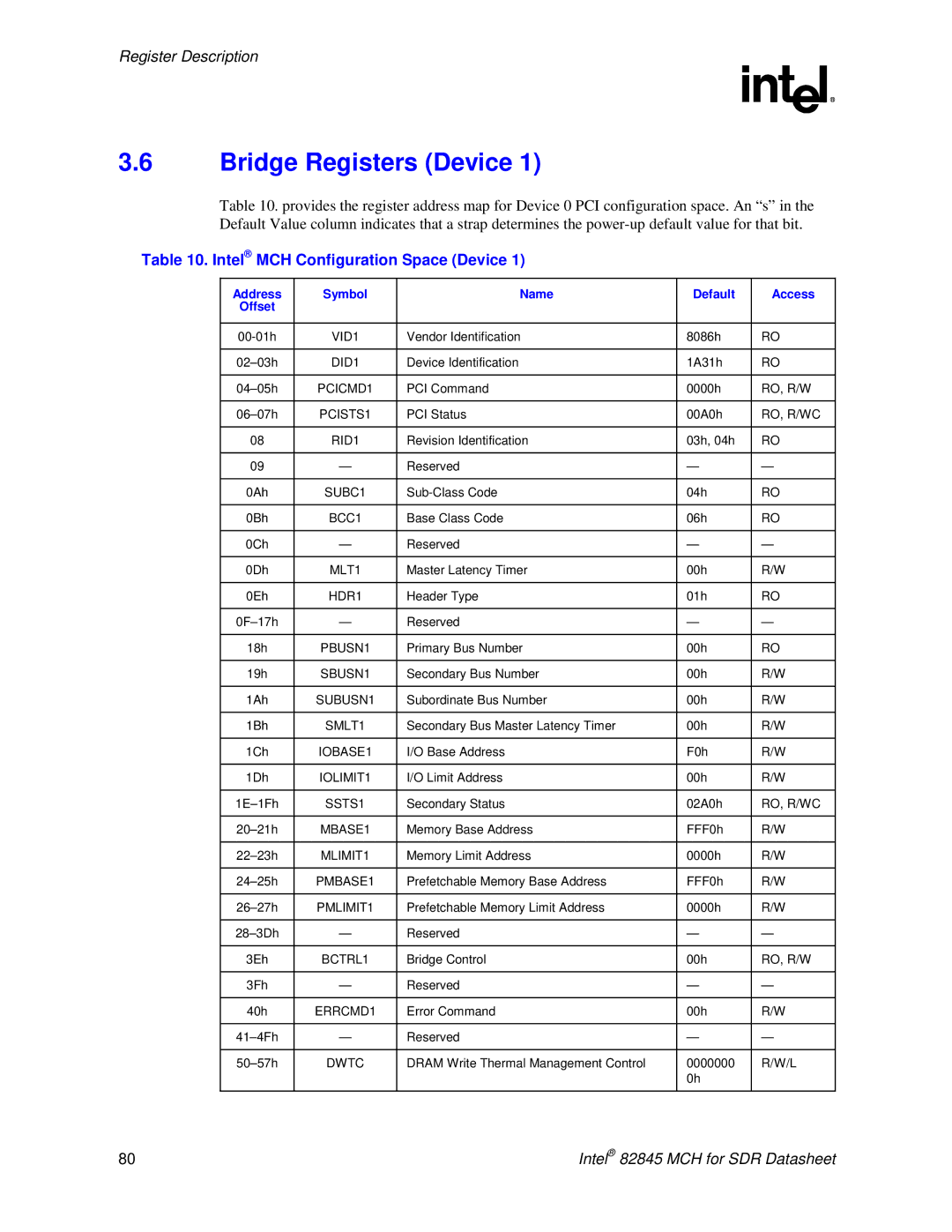
3.6Bridge Registers (Device 1)
Table 10. provides the register address map for Device 0 PCI configuration space. An “s” in the Default Value column indicates that a strap determines the
Table 10. Intel® MCH Configuration Space (Device 1)
Address | Symbol | Name | Default | Access |
Offset |
|
|
|
|
|
|
|
|
|
VID1 | Vendor Identification | 8086h | RO | |
|
|
|
|
|
DID1 | Device Identification | 1A31h | RO | |
|
|
|
|
|
PCICMD1 | PCI Command | 0000h | RO, R/W | |
|
|
|
|
|
PCISTS1 | PCI Status | 00A0h | RO, R/WC | |
|
|
|
|
|
08 | RID1 | Revision Identification | 03h, 04h | RO |
|
|
|
|
|
09 | — | Reserved | — | — |
|
|
|
|
|
0Ah | SUBC1 | 04h | RO | |
|
|
|
|
|
0Bh | BCC1 | Base Class Code | 06h | RO |
|
|
|
|
|
0Ch | — | Reserved | — | — |
|
|
|
|
|
0Dh | MLT1 | Master Latency Timer | 00h | R/W |
|
|
|
|
|
0Eh | HDR1 | Header Type | 01h | RO |
|
|
|
|
|
— | Reserved | — | — | |
|
|
|
|
|
18h | PBUSN1 | Primary Bus Number | 00h | RO |
|
|
|
|
|
19h | SBUSN1 | Secondary Bus Number | 00h | R/W |
|
|
|
|
|
1Ah | SUBUSN1 | Subordinate Bus Number | 00h | R/W |
|
|
|
|
|
1Bh | SMLT1 | Secondary Bus Master Latency Timer | 00h | R/W |
|
|
|
|
|
1Ch | IOBASE1 | I/O Base Address | F0h | R/W |
|
|
|
|
|
1Dh | IOLIMIT1 | I/O Limit Address | 00h | R/W |
|
|
|
|
|
SSTS1 | Secondary Status | 02A0h | RO, R/WC | |
|
|
|
|
|
MBASE1 | Memory Base Address | FFF0h | R/W | |
|
|
|
|
|
MLIMIT1 | Memory Limit Address | 0000h | R/W | |
|
|
|
|
|
PMBASE1 | Prefetchable Memory Base Address | FFF0h | R/W | |
|
|
|
|
|
PMLIMIT1 | Prefetchable Memory Limit Address | 0000h | R/W | |
|
|
|
|
|
— | Reserved | — | — | |
|
|
|
|
|
3Eh | BCTRL1 | Bridge Control | 00h | RO, R/W |
|
|
|
|
|
3Fh | — | Reserved | — | — |
|
|
|
|
|
40h | ERRCMD1 | Error Command | 00h | R/W |
|
|
|
|
|
— | Reserved | — | — | |
|
|
|
|
|
DWTC | DRAM Write Thermal Management Control | 0000000 | R/W/L | |
|
|
| 0h |
|
|
|
|
|
|
80 | Intel® 82845 MCH for SDR Datasheet |