Register Description
R
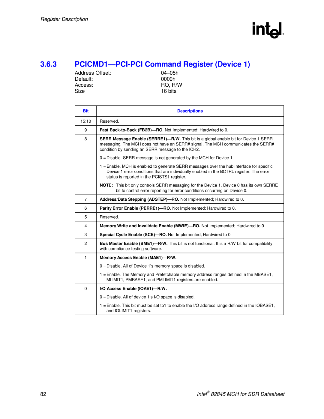
3.6.3PCICMD1—PCI-PCI Command Register (Device 1)
Address Offset: |
| |
Default: |
| 0000h |
Access: |
| RO, R/W |
Size |
| 16 bits |
|
|
|
Bit |
| Descriptions |
|
|
|
15:10 | Reserved. |
|
|
| |
9 | Fast | |
|
| |
8 | SERR Message Enable | |
| messaging. The MCH does not have an SERR# signal. The MCH communicates the SERR# | |
| condition by sending an SERR message to the ICH2. | |
| 0 = Disable. SERR message is not generated by the MCH for Device 1. | |
| 1 = Enable. MCH is enabled to generate SERR messages over the hub interface for specific | |
| Device 1 error conditions that are individually enabled in the BCTRL register. The error | |
| status is reported in the PCISTS1 register. | |
| NOTE: This bit only controls SERR messaging for the Device 1. Device 0 has its own SERRE | |
| bit to control error reporting for error conditions occurring on Device 0. | |
|
| |
7 | Address/Data Stepping | |
|
| |
6 | Parity Error Enable | |
|
|
|
5 | Reserved. |
|
|
| |
4 | Memory Write and Invalidate Enable | |
|
| |
3 | Special Cycle Enable | |
|
| |
2 | Bus Master Enable | |
| with compliance testing software. | |
|
| |
1 | Memory Access Enable | |
| 0 = Disable. All of Device 1’s memory space is disabled. | |
| 1 = Enable. The Memory and Prefetchable memory address ranges defined in the MBASE1, | |
| MLIMIT1, PMBASE1, and PMLIMIT1 registers are enabled. | |
|
| |
0 | I/O Access Enable | |
| 0 = Disable. All of device 1’s I/O space is disabled. | |
| 1 = Enable. This bit must be set to1 to enable the I/O address range defined in the IOBASE1, | |
| and IOLIMIT1 registers. |
|
|
|
|
82 | Intel® 82845 MCH for SDR Datasheet |