Register Description
R
3.5.23SMRAM—System Management RAM Control Register (Device 0)
Address Offset: | 9Dh |
Default Value: | 02h |
Access: | R/W, RO, R/W/L |
Size: | 8 bits |
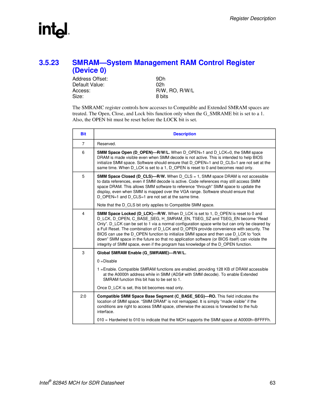
The SMRAMC register controls how accesses to Compatible and Extended SMRAM spaces are treated. The Open, Close, and Lock bits function only when the G_SMRAME bit is set to a 1. Also, the OPEN bit must be reset before the LOCK bit is set.
Bit | Description |
|
|
7 | Reserved. |
|
|
6 | SMM Space Open |
| DRAM is made visible even when SMM decode is not active. This is intended to help BIOS |
| initialize SMM space. Software should ensure that D_OPEN=1 and D_CLS=1 are not set at the |
| same time. When D_LCK is set to a 1, D_OPEN is reset to 0 and becomes read only. |
|
|
5 | SMM Space Closed |
| to data references, even if SMM decode is active. Code references may still access SMM |
| space DRAM. This allows SMM software to reference “through” SMM space to update the |
| display, even when SMM is mapped over the VGA range. Software should ensure that |
| D_OPEN=1 and D_CLS=1 are not set at the same time. |
| Note that the D_CLS bit only applies to Compatible SMM space. |
|
|
4 | SMM Space Locked |
| D_LCK, D_OPEN, C_BASE_SEG, H_SMRAM_EN, TSEG_SZ and TSEG_EN become “Read |
| Only”. D_LCK can be set to 1 via a normal configuration space write but can only be cleared by |
| a Full Reset. The combination of D_LCK and D_OPEN provide convenience with security. The |
| BIOS can use the D_OPEN function to initialize SMM space and then use D_LCK to “lock |
| down” SMM space in the future so that no application software (or BIOS itself) can violate the |
| integrity of SMM space, even if the program has knowledge of the D_OPEN function. |
|
|
3 | Global SMRAM Enable |
| 0 =Disable |
| 1 =Enable. Compatible SMRAM functions are enabled, providing 128 KB of DRAM accessible |
| at the A0000h address while in SMM (ADS# with SMM decode). To enable Extended |
| SMRAM function this bit has to be set to 1. |
| Once D_LCK is set, this bit becomes read only. |
|
|
2:0 | Compatible SMM Space Base Segment |
| location of SMM space. “SMM DRAM” is not remapped. It is simply “made visible” if the |
| conditions are right to access SMM space, otherwise the access is forwarded to the hub |
| interface. |
| 010 = Hardwired to 010 to indicate that the MCH supports the SMM space at |
|
|
Intel® 82845 MCH for SDR Datasheet | 63 |
