Telecom
12.0Telecom Clock
12.1Functional Description
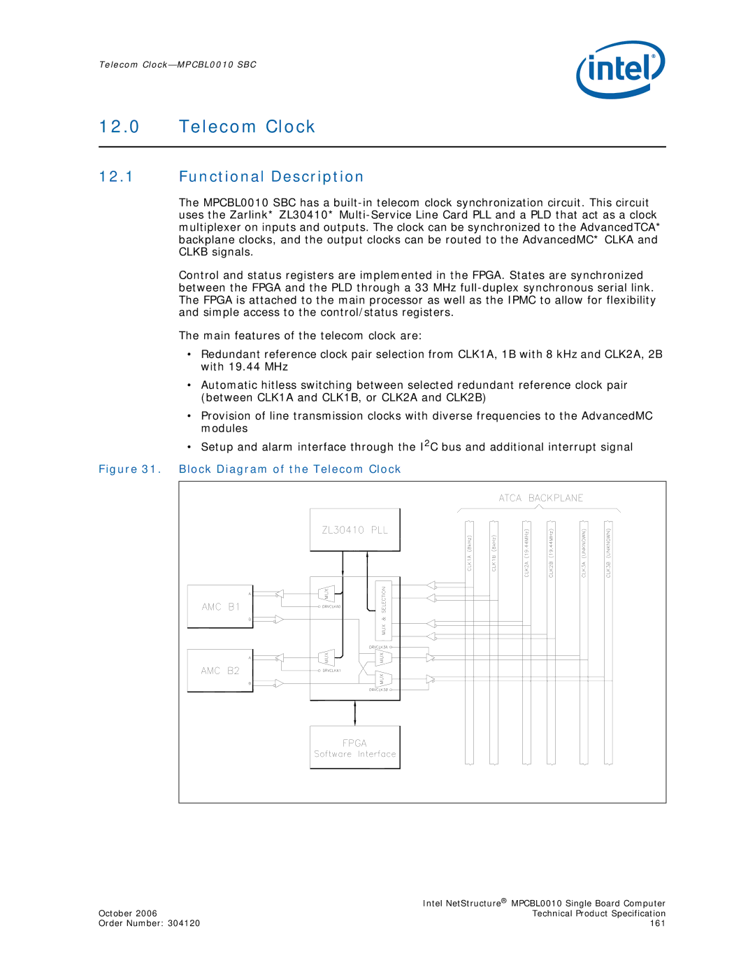
The MPCBL0010 SBC has a
Control and status registers are implemented in the FPGA. States are synchronized between the FPGA and the PLD through a 33 MHz
The main features of the telecom clock are:
•Redundant reference clock pair selection from CLK1A, 1B with 8 kHz and CLK2A, 2B with 19.44 MHz
•Automatic hitless switching between selected redundant reference clock pair (between CLK1A and CLK1B, or CLK2A and CLK2B)
•Provision of line transmission clocks with diverse frequencies to the AdvancedMC modules
•Setup and alarm interface through the I2C bus and additional interrupt signal
Figure 31. Block Diagram of the Telecom Clock
| Intel NetStructure® MPCBL0010 Single Board Computer |
October 2006 | Technical Product Specification |
Order Number: 304120 | 161 |