MPCBL0010
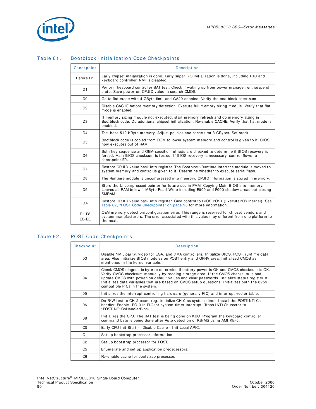
Table 61. | Bootblock Initialization Code Checkpoints | |
|
|
|
| Checkpoint | Description |
|
|
|
| Before D1 | Early chipset initialization is done. Early super I/O initialization is done, including RTC and |
| keyboard controller. NMI is disabled. | |
|
| |
|
|
|
| D1 | Perform keyboard controller BAT test. Check if waking up from power management suspend |
| state. Save | |
|
| |
|
|
|
| D0 | Go to flat mode with 4 GByte limit and GA20 enabled. Verify the bootblock checksum. |
|
|
|
| D2 | Disable CACHE before memory detection. Execute full memory sizing module. Verify that flat |
| mode is enabled. | |
|
| |
|
|
|
|
| If memory sizing module not executed, start memory refresh and do memory sizing in |
| D3 | Bootblock code. Do additional chipset initialization. |
|
| enabled. |
|
|
|
| D4 | Test base 512 KByte memory. Adjust policies and cache first 8 GBytes. Set stack. |
|
|
|
| D5 | Bootblock code is copied from ROM to lower system memory and control is given to it. BIOS |
| now executes out of RAM. | |
|
| |
|
|
|
|
| Both key sequence and |
| D6 | forced. Main BIOS checksum is tested. If BIOS recovery is necessary, control flows to |
|
| checkpoint E0. |
|
|
|
| D7 | Restore CPUID value back into register. The |
| system memory and control is given to it. Determine whether to execute serial flash. | |
|
| |
|
|
|
| D8 | The Runtime module is uncompressed into memory. CPUID information is stored in memory. |
|
|
|
|
| Store the Uncompressed pointer for future use in PMM. Copying Main BIOS into memory. |
| D9 | Leaves all RAM below 1 MByte |
|
| SMRAM. |
|
|
|
| DA | Restore CPUID value back into register. Give control to BIOS POST (ExecutePOSTKernel). See |
| Table 62, “POST Code Checkpoints” on page 90 for more information. | |
|
| |
|
|
|
| OEM memory detection/configuration error. This range is reserved for chipset vendors and | |
| system manufacturers. The error associated with this value may different from one platform to | |
| ||
| the next. | |
|
| |
|
|
|
Table 62. | POST Code Checkpoints | |
|
|
|
| Checkpoint | Description |
|
|
|
|
| Disable NMI, parity, video for EGA, and DMA controllers. Initialize BIOS, POST, runtime data |
| 03 | area. Also initialize BIOS modules on POST entry and GPNV area. Initialized CMOS as |
|
| mentioned in the kernel variable. |
|
|
|
|
| Check CMOS diagnostic byte to determine if battery power is OK and CMOS checksum is OK. |
|
| Verify CMOS checksum manually by reading storage area. If the CMOS checksum is bad, |
| 04 | update CMOS with |
|
| Initializes data variables that are based on CMOS setup questions. Initializes both the 8259 |
|
| compatible PICs in the system. |
|
|
|
| 05 | Initializes the interrupt controlling hardware (generally PIC) and interrupt vector table. |
|
|
|
|
| Do R/W test to |
| 06 | handler. Enable |
|
| “POSTINT1ChHandlerBlock.” |
|
|
|
| 08 | Initializes the CPU. The BAT test is being done on KBC. Program the keyboard controller |
| command byte is being done after Auto detection of KB/MS using AMI | |
|
| |
|
|
|
| C0 | Early CPU Init Start |
|
|
|
| C1 | Set up bootstrap processor information. |
|
|
|
| C2 | Set up bootstrap processor for POST. |
|
|
|
| C5 | Enumerate and set up application predecessors. |
|
|
|
| C6 | |
|
|
|
Intel NetStructure® MPCBL0010 Single Board Computer |
|
Technical Product Specification | October 2006 |
90 | Order Number: 304120 |