Telecom
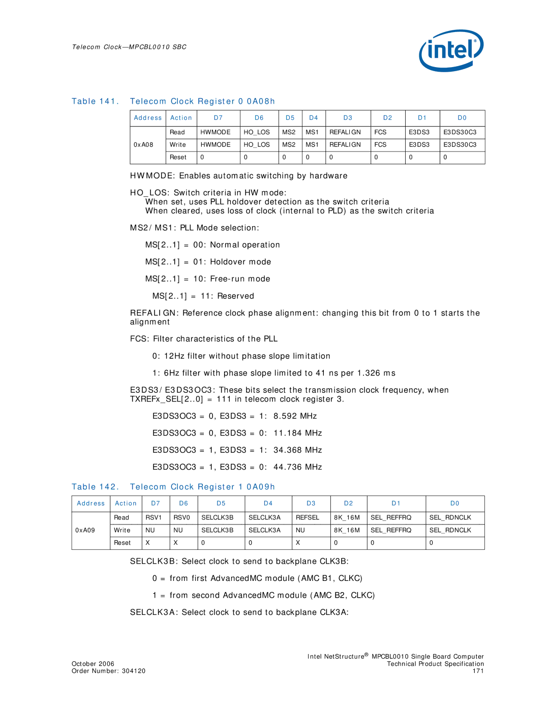
Table 141. Telecom Clock Register 0 0A08h
Address | Action | D7 | D6 | D5 | D4 | D3 | D2 | D1 | D0 |
|
|
|
|
|
|
|
|
|
|
| Read | HWMODE | HO_LOS | MS2 | MS1 | REFALIGN | FCS | E3DS3 | E3DS30C3 |
|
|
|
|
|
|
|
|
|
|
0xA08 | Write | HWMODE | HO_LOS | MS2 | MS1 | REFALIGN | FCS | E3DS3 | E3DS30C3 |
|
|
|
|
|
|
|
|
|
|
| Reset | 0 | 0 | 0 | 0 | 0 | 0 | 0 | 0 |
|
|
|
|
|
|
|
|
|
|
HWMODE: Enables automatic switching by hardware
HO_LOS: Switch criteria in HW mode:
When set, uses PLL holdover detection as the switch criteria
When cleared, uses loss of clock (internal to PLD) as the switch criteria
MS2/MS1: PLL Mode selection:
MS[2..1] = 00: Normal operation
MS[2..1] = 01: Holdover mode
MS[2..1] = 10:
MS[2..1] = 11: Reserved
REFALIGN: Reference clock phase alignment: changing this bit from 0 to 1 starts the alignment
FCS: Filter characteristics of the PLL
0:12Hz filter without phase slope limitation
1:6Hz filter with phase slope limited to 41 ns per 1.326 ms
E3DS3/E3DS3OC3: These bits select the transmission clock frequency, when TXREFx_SEL[2..0] = 111 in telecom clock register 3.
E3DS3OC3 = 0, E3DS3 = 1: 8.592 MHz
E3DS3OC3 = 0, E3DS3 = 0: 11.184 MHz
E3DS3OC3 = 1, E3DS3 = 1: 34.368 MHz
E3DS3OC3 = 1, E3DS3 = 0: 44.736 MHz
Table 142. Telecom Clock Register 1 0A09h
Address | Action | D7 | D6 | D5 | D4 | D3 | D2 | D1 | D0 |
|
|
|
|
|
|
|
|
|
|
| Read | RSV1 | RSV0 | SELCLK3B | SELCLK3A | REFSEL | 8K_16M | SEL_REFFRQ | SEL_RDNCLK |
|
|
|
|
|
|
|
|
|
|
0xA09 | Write | NU | NU | SELCLK3B | SELCLK3A | NU | 8K_16M | SEL_REFFRQ | SEL_RDNCLK |
|
|
|
|
|
|
|
|
|
|
| Reset | X | X | 0 | 0 | X | 0 | 0 | 0 |
|
|
|
|
|
|
|
|
|
|
SELCLK3B: Select clock to send to backplane CLK3B:
0 = from first AdvancedMC module (AMC B1, CLKC)
1 = from second AdvancedMC module (AMC B2, CLKC) SELCLK3A: Select clock to send to backplane CLK3A:
| Intel NetStructure® MPCBL0010 Single Board Computer |
October 2006 | Technical Product Specification |
Order Number: 304120 | 171 |
