MPCBL0010
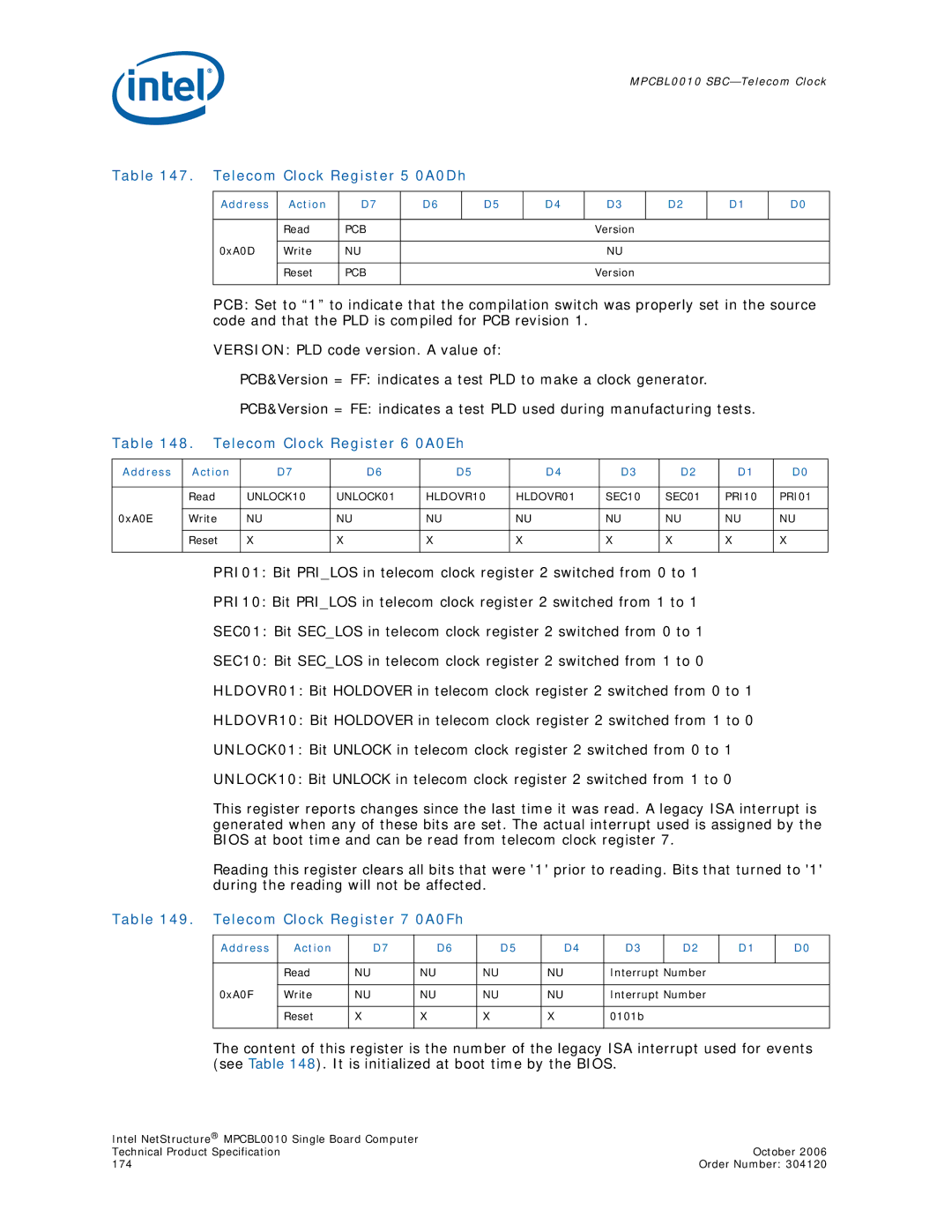
Table 147. Telecom Clock Register 5 0A0Dh
Address | Action | D7 | D6 | D5 | D4 | D3 | D2 | D1 | D0 |
|
|
|
|
|
|
|
|
|
|
| Read | PCB |
|
|
| Version |
|
|
|
|
|
|
|
|
|
|
|
|
|
0xA0D | Write | NU |
|
|
| NU |
|
|
|
|
|
|
|
|
|
|
|
|
|
| Reset | PCB |
|
|
| Version |
|
|
|
|
|
|
|
|
|
|
|
|
|
PCB: Set to “1” to indicate that the compilation switch was properly set in the source code and that the PLD is compiled for PCB revision 1.
VERSION: PLD code version. A value of:
PCB&Version = FF: indicates a test PLD to make a clock generator.
PCB&Version = FE: indicates a test PLD used during manufacturing tests.
Table 148. Telecom Clock Register 6 0A0Eh
Address | Action | D7 | D6 | D5 | D4 | D3 | D2 | D1 | D0 |
|
|
|
|
|
|
|
|
|
|
| Read | UNLOCK10 | UNLOCK01 | HLDOVR10 | HLDOVR01 | SEC10 | SEC01 | PRI10 | PRI01 |
|
|
|
|
|
|
|
|
|
|
0xA0E | Write | NU | NU | NU | NU | NU | NU | NU | NU |
|
|
|
|
|
|
|
|
|
|
| Reset | X | X | X | X | X | X | X | X |
|
|
|
|
|
|
|
|
|
|
PRI01: Bit PRI_LOS in telecom clock register 2 switched from 0 to 1
PRI10: Bit PRI_LOS in telecom clock register 2 switched from 1 to 1
SEC01: Bit SEC_LOS in telecom clock register 2 switched from 0 to 1
SEC10: Bit SEC_LOS in telecom clock register 2 switched from 1 to 0
HLDOVR01: Bit HOLDOVER in telecom clock register 2 switched from 0 to 1
HLDOVR10: Bit HOLDOVER in telecom clock register 2 switched from 1 to 0
UNLOCK01: Bit UNLOCK in telecom clock register 2 switched from 0 to 1
UNLOCK10: Bit UNLOCK in telecom clock register 2 switched from 1 to 0
This register reports changes since the last time it was read. A legacy ISA interrupt is generated when any of these bits are set. The actual interrupt used is assigned by the BIOS at boot time and can be read from telecom clock register 7.
Reading this register clears all bits that were '1' prior to reading. Bits that turned to '1' during the reading will not be affected.
Table 149. Telecom Clock Register 7 0A0Fh
Address | Action | D7 | D6 | D5 | D4 | D3 | D2 | D1 | D0 |
|
|
|
|
|
|
|
|
|
|
| Read | NU | NU | NU | NU | Interrupt Number |
|
| |
|
|
|
|
|
|
|
|
| |
0xA0F | Write | NU | NU | NU | NU | Interrupt Number |
|
| |
|
|
|
|
|
|
|
|
|
|
| Reset | X | X | X | X | 0101b |
|
|
|
|
|
|
|
|
|
|
|
|
|
The content of this register is the number of the legacy ISA interrupt used for events (see Table 148). It is initialized at boot time by the BIOS.
Intel NetStructure® MPCBL0010 Single Board Computer |
|
Technical Product Specification | October 2006 |
174 | Order Number: 304120 |