MPCBL0010
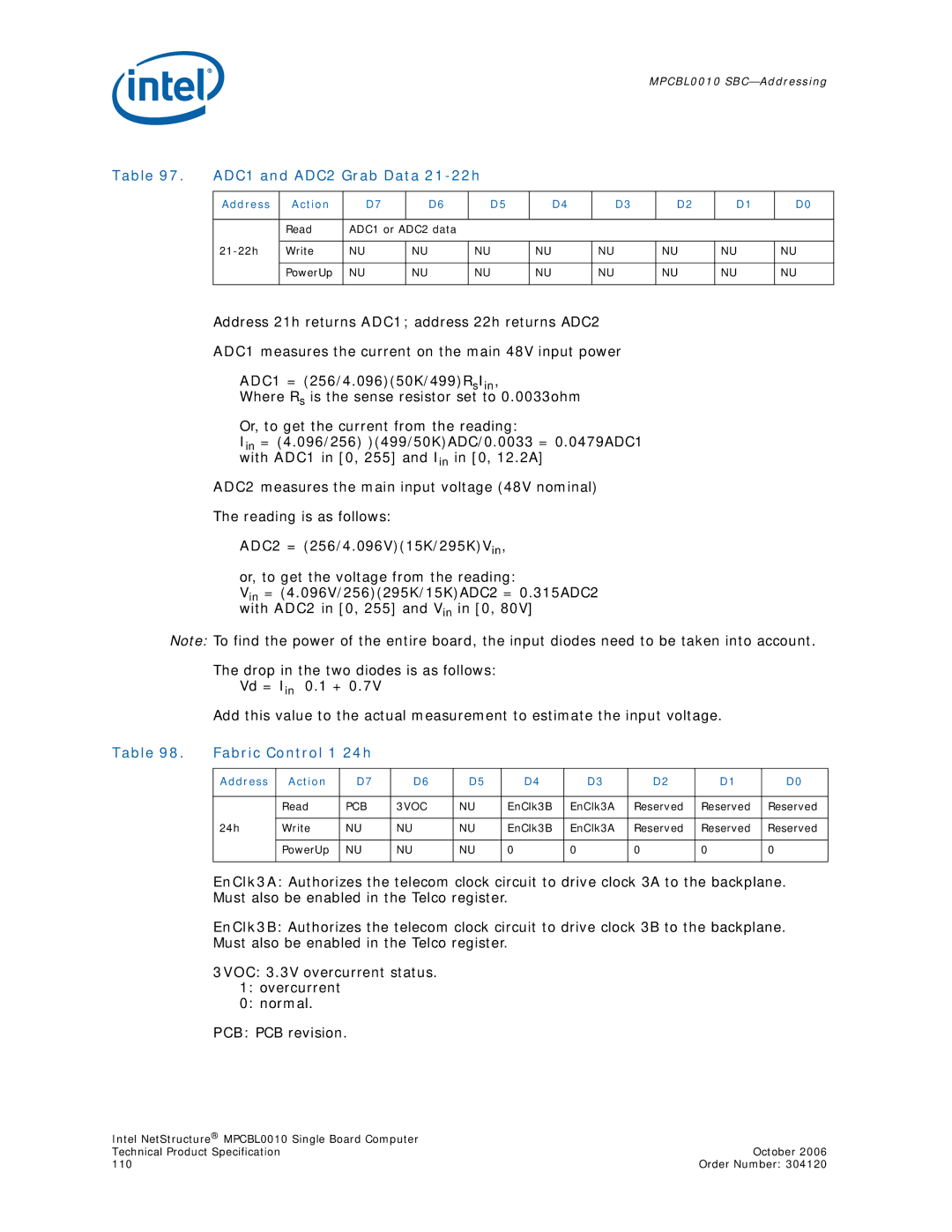
Table 97. ADC1 and ADC2 Grab Data 21-22h
Address | Action | D7 | D6 | D5 | D4 | D3 | D2 | D1 | D0 |
|
|
|
|
|
|
|
|
|
|
| Read | ADC1 or ADC2 data |
|
|
|
|
|
| |
|
|
|
|
|
|
|
|
|
|
Write | NU | NU | NU | NU | NU | NU | NU | NU | |
|
|
|
|
|
|
|
|
|
|
| PowerUp | NU | NU | NU | NU | NU | NU | NU | NU |
|
|
|
|
|
|
|
|
|
|
Address 21h returns ADC1; address 22h returns ADC2
ADC1 measures the current on the main 48V input power
ADC1 = (256/4.096)(50K/499)RsIin,
Where Rs is the sense resistor set to 0.0033ohm
Or, to get the current from the reading:
Iin = (4.096/256) )(499/50K)ADC/0.0033 = 0.0479ADC1 with ADC1 in [0, 255] and Iin in [0, 12.2A]
ADC2 measures the main input voltage (48V nominal)
The reading is as follows:
ADC2 = (256/4.096V)(15K/295K)Vin,
or, to get the voltage from the reading:
Vin = (4.096V/256)(295K/15K)ADC2 = 0.315ADC2 with ADC2 in [0, 255] and Vin in [0, 80V]
Note: To find the power of the entire board, the input diodes need to be taken into account.
The drop in the two diodes is as follows:
Vd = Iin 0.1 + 0.7V
Add this value to the actual measurement to estimate the input voltage.
Table 98. | Fabric Control 1 24h |
|
|
|
|
|
|
| ||
|
|
|
|
|
|
|
|
|
|
|
| Address | Action | D7 | D6 | D5 | D4 | D3 | D2 | D1 | D0 |
|
|
|
|
|
|
|
|
|
|
|
|
| Read | PCB | 3VOC | NU | EnClk3B | EnClk3A | Reserved | Reserved | Reserved |
|
|
|
|
|
|
|
|
|
|
|
| 24h | Write | NU | NU | NU | EnClk3B | EnClk3A | Reserved | Reserved | Reserved |
|
|
|
|
|
|
|
|
|
|
|
|
| PowerUp | NU | NU | NU | 0 | 0 | 0 | 0 | 0 |
|
|
|
|
|
|
|
|
|
|
|
EnClk3A: Authorizes the telecom clock circuit to drive clock 3A to the backplane. Must also be enabled in the Telco register.
EnClk3B: Authorizes the telecom clock circuit to drive clock 3B to the backplane. Must also be enabled in the Telco register.
3VOC: 3.3V overcurrent status.
1:overcurrent
0:normal.
PCB: PCB revision.
Intel NetStructure® MPCBL0010 Single Board Computer |
|
Technical Product Specification | October 2006 |
110 | Order Number: 304120 |
