MPCBL0010 SBC—Feature Overview
Note: Two
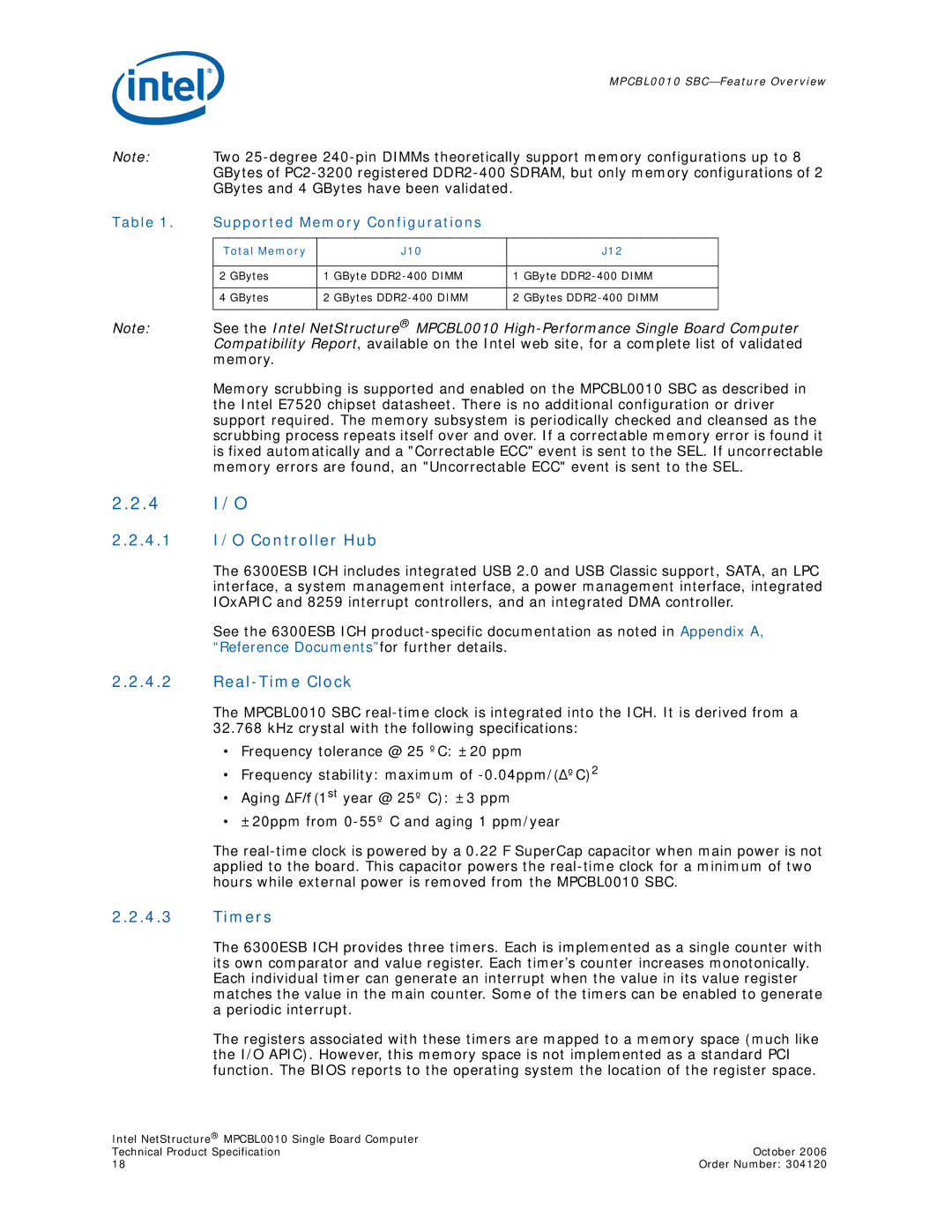
Table 1. | Supported Memory Configurations |
|
|
| ||
|
|
|
|
|
|
|
| Total Memory |
| J10 |
| J12 |
|
|
|
|
|
|
| |
| 2 GBytes | 1 | GByte | 1 | GByte | |
|
|
|
|
|
|
|
| 4 GBytes | 2 | GBytes | 2 | GBytes | DIMM |
|
|
|
|
|
|
|
Note: See the Intel NetStructure® MPCBL0010
Memory scrubbing is supported and enabled on the MPCBL0010 SBC as described in the Intel E7520 chipset datasheet. There is no additional configuration or driver support required. The memory subsystem is periodically checked and cleansed as the scrubbing process repeats itself over and over. If a correctable memory error is found it is fixed automatically and a "Correctable ECC" event is sent to the SEL. If uncorrectable memory errors are found, an "Uncorrectable ECC" event is sent to the SEL.
2.2.4I/O
2.2.4.1I/O Controller Hub
The 6300ESB ICH includes integrated USB 2.0 and USB Classic support, SATA, an LPC interface, a system management interface, a power management interface, integrated IOxAPIC and 8259 interrupt controllers, and an integrated DMA controller.
See the 6300ESB ICH
2.2.4.2Real-Time Clock
The MPCBL0010 SBC
32.768 kHz crystal with the following specifications:
•Frequency tolerance @ 25 ºC: ±20 ppm
•Frequency stability: maximum of
•Aging ΔF/f (1st year @ 25º C): ±3 ppm
•±20ppm from
The
2.2.4.3Timers
The 6300ESB ICH provides three timers. Each is implemented as a single counter with its own comparator and value register. Each timer’s counter increases monotonically. Each individual timer can generate an interrupt when the value in its value register matches the value in the main counter. Some of the timers can be enabled to generate a periodic interrupt.
The registers associated with these timers are mapped to a memory space (much like the I/O APIC). However, this memory space is not implemented as a standard PCI function. The BIOS reports to the operating system the location of the register space.
Intel NetStructure® MPCBL0010 Single Board Computer |
|
Technical Product Specification | October 2006 |
18 | Order Number: 304120 |