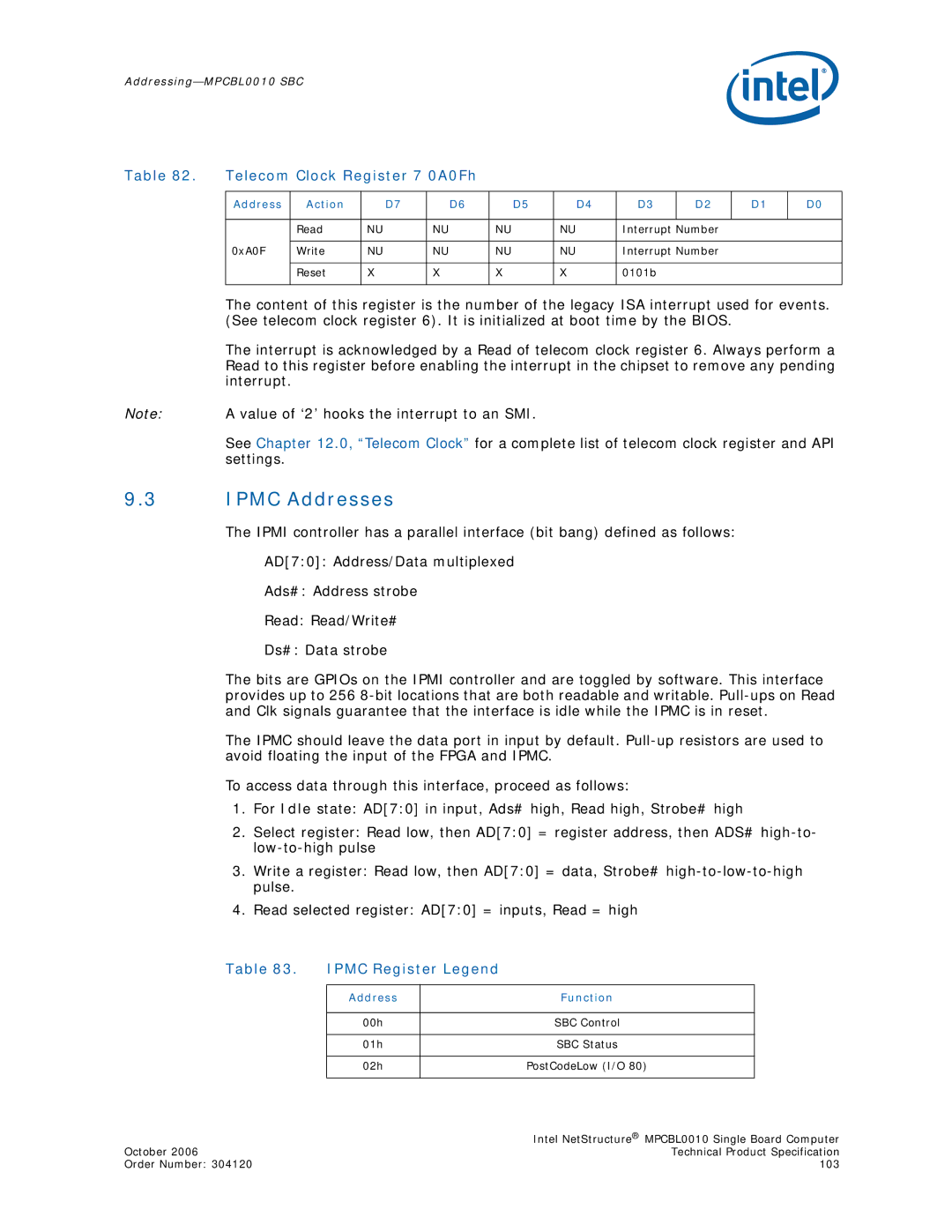
Table 82. | Telecom Clock Register 7 0A0Fh |
|
|
|
|
|
| |||
|
|
|
|
|
|
|
|
|
|
|
| Address | Action | D7 | D6 | D5 | D4 | D3 | D2 | D1 | D0 |
|
|
|
|
|
|
|
|
|
|
|
|
| Read | NU | NU | NU | NU | Interrupt Number |
|
| |
|
|
|
|
|
|
|
|
|
| |
| 0xA0F | Write | NU | NU | NU | NU | Interrupt Number |
|
| |
|
|
|
|
|
|
|
|
|
|
|
|
| Reset | X | X | X | X | 0101b |
|
|
|
|
|
|
|
|
|
|
|
|
|
|
The content of this register is the number of the legacy ISA interrupt used for events. (See telecom clock register 6). It is initialized at boot time by the BIOS.
The interrupt is acknowledged by a Read of telecom clock register 6. Always perform a Read to this register before enabling the interrupt in the chipset to remove any pending interrupt.
Note: A value of ‘2’ hooks the interrupt to an SMI.
See Chapter 12.0, “Telecom Clock” for a complete list of telecom clock register and API settings.
9.3IPMC Addresses
The IPMI controller has a parallel interface (bit bang) defined as follows:
AD[7:0]: Address/Data multiplexed
Ads#: Address strobe
Read: Read/Write#
Ds#: Data strobe
The bits are GPIOs on the IPMI controller and are toggled by software. This interface provides up to 256
The IPMC should leave the data port in input by default.
To access data through this interface, proceed as follows:
1.For Idle state: AD[7:0] in input, Ads# high, Read high, Strobe# high
2.Select register: Read low, then AD[7:0] = register address, then ADS#
3.Write a register: Read low, then AD[7:0] = data, Strobe#
4.Read selected register: AD[7:0] = inputs, Read = high
Table 83. | IPMC Register Legend |
| |
|
|
|
|
| Address |
| Function |
|
|
|
|
| 00h |
| SBC Control |
|
|
|
|
| 01h |
| SBC Status |
|
|
|
|
| 02h |
| PostCodeLow (I/O 80) |
|
|
|
|
| Intel NetStructure® MPCBL0010 Single Board Computer |
October 2006 | Technical Product Specification |
Order Number: 304120 | 103 |