MCF51QE64 MCF51QE32
Page
MCF51QE128 Series Features
Page
MCF51QE128 Reference Manual
MCF51QE128 MCU Series Reference Manual, Rev
Contents
Section Number Title
Freescale Semiconductor
Chapter Resets, Interrupts, and General System Control
Title Chapter Parallel Input/Output Control
127
ColdFire Core
Chapter Interrupt Controller CF1INTC
Analog Comparator 3V ACMPVLPV1
11.1.5
Internal Clock Source S08ICSV3
Chapter Inter-Integrated Circuit S08IICV2
Section Number Title
Real-Time Counter S08RTCV1
Serial Peripheral Interface S08SPIV3
Chapter Timer/Pulse-Width Modulator S08TPMV3
Chapter Version 1 ColdFire Debug CF1DEBUG
Appendix a Revision History
Feature MCF51QE128
MCF51QE128 Series Features by MCU and Package
Chapter Device Overview
Devices in the MCF51QE128/64/32 Series
Xosc
MCU Block Diagram
MCF51QE128/64/32 Block Diagram
System Clocks
V1 ColdFire Core
Internal Clock Source ICS Module
Module Versions
System Clock Distribution
Simplified ICS Block Diagram
Icsirclk
ICS Modes of Operation
FLL Bypassed Internal Low-Power Fbilp
FLL Engaged Internal FEI
FLL Engaged External FEE
Stop Stop
FLL Bypassed External Low-Power Fbelp
Get the latest version from freescale.com
Get the latest version from freescale.com
Device Pin Assignment
Chapter Pins and Connections
Pin Lqfp
Pins in bold are added from the next smaller package
Recommended System Connections
Basic System Connections
Oscillator
Power
Reset and Rsto
Background / Mode Select BKGD/MS
General-Purpose I/O and Peripheral Ports
ADC Reference Pins VREFH, Vrefl
Pin
Pin Assignment by Package and Pin Sharing Priority
Priority
Number Port Pin Alt
Port Pin Alt
Number
Get the latest version from freescale.com
Introduction
Features
Chapter Modes of Operation
Overview
MCF51QE128/64/32 Power Modes Conceptual Drawing
PMC
CPU / Power Mode Selections
Stop3
Mode Regulator State
Full On
Run Stop2 LPrun
Transition # From Trigger
Triggers for Transitions Shown in Figure
Secure Mode
Debug Mode
Low-Power Run Mode LPrun
Run Mode
BDM in Low-Power Run Mode
Run Modes
Low-Power Wait Mode LPwait
Wait Mode
BDM in Low-Power Wait Mode
Wait Modes
Stop2 Mode
Low-Range Oscillator Considerations for Stop2
Stop3 Mode
Stop4 Low Voltage Detect or BDM Enabled in Stop Mode
Low-Power Mode Behavior
On-Chip Peripheral Modules in Stop and Low-Power Modes
Abbreviations used in Table
CF1CORE
COP
BDC
ICS
IRQ
Get the latest version from freescale.com
Get the latest version from freescale.com
MCF51QE128/64/32 Memory Map
Chapter Memory
Kbytes
RAM
Register Addresses and Bit Assignments
CPU Access Type Allowed by Region
Read Write Base Address Region Byte
Long Byte
ColdFire Memory Organization
Direct-Page Register Summary Sheet 1
Register Address Name
Direct-Page Register Summary Sheet 2
Direct-Page Register Summary Sheet 3
High-Page Register Summary Sheet 1
Direct-Page Register Summary Sheet 4
High-Page Register Summary Sheet 2
High-Page Register Summary Sheet 3
High-Page Register Summary Sheet 4
High-Page Register Summary Sheet 5
Flash Module Reserved Memory Locations
Reserved Flash Memory Addresses
0x0 0x1 0x2 0x3
0x0000040C
0x0 0x1 0x2 0x3 0x00000408
Reserved Flash Memory Addresses Register
Nvprot
ColdFire Interrupt Controller Memory Map
ColdFire Rapid Gpio Memory Map
V1 ColdFire Rapid Gpio Memory Map
V1 ColdFire Interrupt Controller Memory Map
Flash
RAM
Intcsfrc
Intccfrc
Addresses Desired Value Values Programmed
Features
Lov-Voltage Programming Sequence Example
Flash Clock Divider Register Fcdiv
Register Descriptions
Flash Options Register Fopt and Nvopt
Fcdiv Field Descriptions
10. Fopt Field Descriptions
Flash Configuration Register Fcnfg
11. Fcnfg Field Descriptions
Flash Protection Register Fprot and Nvprot
12. Fprot Field Descriptions
13. Flash Protection Address Range
0x40
0x00-0x3F
0x41 0x00000-0x1EFFF
0x42
Flash Status Register Fstat
Command buffers are full
Fcbef Fccf Fpviol Faccerr Fblank
W1c
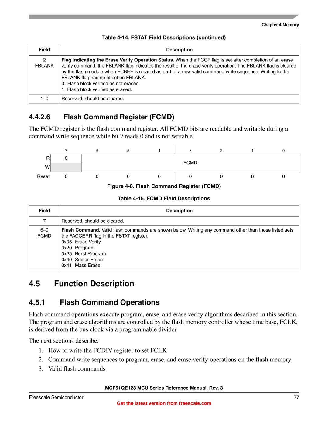
Flash Command Register Fcmd
Flash Command Operations
Function Description
15. Fcmd Field Descriptions
200 195 ⎟ 200 = 3%
Writing the Fcdiv Register
Commands Impossible
Command Write Sequence
Start
ALL Program and Erase
Erase Verify Command
Flash Commands
16. Flash Command Description
Fcmd NVM
Program Command
11. Example Program Command Flow
Burst Program Command
Command Buffer Empty
Sector Erase Command
Sequential
Programming
13. Example Sector Erase Command Flow
14. Example Mass Erase Command Flow
Mass Erase Command
Illegal Flash Operations
Flash Access Violations
Background Debug Mode
Wait Mode
Operating Modes
Flash Protection Violations
Security
Unsecuring the MCU using Backdoor Key Access
Flash Reset Sequence
Resets
Reset While Flash Command Active
Program and Erase Times
Security
Set PRDIV8 and clock divider fields in CSR3
Sync
Stop
Device is unsecure
Microcontroller Reset
Chapter Resets, Interrupts, and General System Control
Computer Operating Properly COP Watchdog
COP Configuration Options
Control Bits Clock Source COP Overflow Count
Copclks Copt
Illegal Address Reset
Illegal Operation Reset
Pin Configuration Options
Interrupts and Exceptions
Low-Voltage Detect LVD System
Power-On Reset Operation
Edge and Level Sensitivity
External Interrupt Initialization
Peripheral Clock Gating
LVD Reset Operation
LVD Interrupt Operation
Low-Voltage Warning LVW Interrupt Operation
Irqsc Register Field Descriptions
Interrupt Pin Request Status and Control Register Irqsc
Irqpdd Irqedg Irqpe Irqf Irqie Irqmod Irqack
Irqpdd
POR
System Reset Status Register SRS
POR LVR
System Options Register 1 SOPT1
SOPT1 Register Field Descriptions
System Options Register 2 SOPT2
SOPT2 Register Field Descriptions
System Device Identification Register SDIDH, Sdidl
SPI1PS SPSCLK1 MOSI1 MISO1 SS1
IIC1PS SDA1 SCL1
Lvdf Lvdie LVDRE2 Lvdse LVDE2 Bgbe Lvdack
Sdidh Register Field Descriptions
Sdidl Register Field Descriptions
LPR Lprs Lpwui Ppde Ppdc Ppdack
SPMSC1 Register Field Descriptions
SPMSC2 Register Field Descriptions
Lvwf Lvdv Lvwv Lvwie
11. LVD and LVW Trip Point Typical Values1
Lvwf
Lvdvlvwv
System Clock Gating Control 2 Register SCGC2
System Clock Gating Control 1 Register SCGC1
12. SCGC1 Register Field Descriptions
TPM3
FLS
13. SCGC2 Register Field Descriptions
RTC SPI2 SPI1
Freescale Semiconductor 109
110 Freescale Semiconductor
Freescale Semiconductor 111
112 Freescale Semiconductor
Freescale Semiconductor 113
Chapter Parallel Input/Output Control
Port Data and Data Direction
Port Slew Rate Enable
Port Internal Pull-up Enable
Pull-up, Slew Rate, and Drive Strength
Data Direction Control Port Data Register Port Read
Freescale Semiconductor 115
Port Data Set, Clear and Toggle Data Registers
Port Drive Strength Select
Keyboard Interrupts
V1 ColdFire Rapid Gpio Functionality
Port Data Set Registers
Port Data Clear Registers
Edge and Level Sensitivity
Edge Only Sensitivity
Pull-up/Pull-down Resistors
Freescale Semiconductor 117
Parallel I/O, Keyboard Interrupt, and Pin Control Registers
Pin Behavior in Stop Modes
Keyboard Interrupt Initialization
Port a Registers
Port a Data Register Ptad
Port a Pull Enable Register Ptape
Port a Data Direction Register Ptadd
PTAD7 PTAD6 PTAD5 PTAD41 PTAD3 PTAD2 PTAD1 PTAD0
Port a Drive Strength Selection Register Ptads
Port a Slew Rate Enable Register Ptase
PTAPE7 PTAPE6 PTAPE5 PTAPE4 PTAPE3 PTAPE2 PTAPE1 PTAPE0
PTASE7 PTASE6 PTASE5 PTASE4 PTASE3 PTASE2 PTASE1 PTASE0
Port B Data Register Ptbd
Port B Registers
Port B Data Direction Register Ptbdd
Ptads Register Field Descriptions
Port B Slew Rate Enable Register Ptbse
Port B Pull Enable Register Ptbpe
Ptbdd Register Field Descriptions
Ptbpe Register Field Descriptions
Port B Drive Strength Selection Register Ptbds
Port C Registers
Port C Data Register Ptcd
10. Ptbds Register Field Descriptions
Port C Data Set Register Ptcset
Port C Data Direction Register Ptcdd
Port C Data Clear Register Ptcclr
12. Ptcdd Register Field Descriptions
Port C Toggle Register Ptctog
Port C Pull Enable Register Ptcpe
14. Ptcclr Register Field Descriptions
16. Ptcpe Register Field Descriptions
Port D Registers
Port C Slew Rate Enable Register Ptcse
Port C Drive Strength Selection Register Ptcds
Port D Data Register Ptdd
Port D Data Direction Register Ptddd
Port D Pull Enable Register Ptdpe
19. Ptdd Register Field Descriptions
20. Ptddd Register Field Descriptions
Port E Registers
Port D Slew Rate Enable Register Ptdse
Port D Drive Strength Selection Register Ptdds
Port E Data Register Pted
Port E Data Set Register Pteset
Port E Data Direction Register Ptedd
24. Pted Register Field Descriptions
25. Ptedd Register Field Descriptions
Port E Data Clear Register Pteclr
Port E Pull Enable Register Ptepe
Port E Toggle Register Ptetog
PTEPE7 PTEPE6 PTEPE5 PTEPE4 PTEPE3 PTEPE2 PTEPE1 PTEPE0
Port E Drive Strength Selection Register Pteds
Port E Slew Rate Enable Register Ptese
29. Ptepe Register Field Descriptions
30. Ptese Register Field Descriptions
Port F Registers
Port F Pull Enable Register Ptfpe
Port F Data Register Ptfd
Port F Data Direction Register Ptfdd
Port F Drive Strength Selection Register Ptfds
Port F Slew Rate Enable Register Ptfse
34. Ptfpe Register Field Descriptions
35. Ptfse Register Field Descriptions
Port G Data Register Ptgd
Port G Registers
Port G Data Direction Register Ptgdd
36. Ptfds Register Field Descriptions
Port G Slew Rate Enable Register Ptgse
Port G Pull Enable Register Ptgpe
Port G Drive Strength Selection Register Ptgds
39. Ptgpe Register Field Descriptions
Port H Data Register Pthd
Port H Registers
Port H Data Direction Register Pthdd
41. Ptgds Register Field Descriptions
Port H Slew Rate Enable Register Pthse
Port H Pull Enable Register Pthpe
Port H Drive Strength Selection Register Pthds
44. Pthpe Register Field Descriptions
Port J Data Direction Register Ptjdd
Port J Registers
Port J Data Register Ptjd
Port J Slew Rate Enable Register Ptjse
Port J Pull Enable Register Ptjpe
Port J Drive Strength Selection Register Ptjds
49. Ptjpe Register Field Descriptions
10.1 KBI1 Interrupt Status and Control Register KBI1SC
Keyboard Interrupt 1 KBI1 Registers
51. Ptjds Register Field Descriptions
52. KBI1 Pin Mapping
10.3 KBI1 Interrupt Edge Select Register KBI1ES
Keyboard Interrupt 1 KBI2 Registers
10.2 KBI1 Interrupt Pin Select Register KBI1PE
11.2 KBI2 Interrupt Pin Select Register KBI2PE
11.1 KBI2 Interrupt Status and Control Register KBI2SC
57. KBI2SC Register Field Descriptions
58. KBI2PE Register Field Descriptions
Freescale Semiconductor 143
11.3 KBI2 Interrupt Edge Select Register KBI2ES
59. KBI2ES Register Field Descriptions
144 Freescale Semiconductor
Overview
Chapter ColdFire Core
Memory Map/Register Description
Supervisor Access Only Registers
Supervisor/User Access Registers
Data Registers D0-D7
ColdFire Core Programming Model
Data
Address Registers A0-A6
Supervisor/User Stack Pointers A7 and OTHERA7
Freescale Semiconductor 149
Condition Code Register CCR
CCR Field Descriptions
Program Counter PC
Vector Base Register VBR
CPU Configuration Register Cpucr
BWD
Status Register SR
SR Field Descriptions
Instruction Set Architecture Isac
Functional Description
Instruction Enhancements over Revision Isaa
Instruction Description
Exception Processing Overview
Assignment Numbers Offset Hex Counter
Exception Vector Assignments
Vector Stacked
Assignment
Exception Stack Frame Definition
Numbers Offset Hex Counter
SSP →
2.2 S08 and ColdFire Exception Processing Comparison
Fault Status Encodings
Format Field Encodings
FS30 Definition
RTI RTE
Exception Processing Comparison
Attribute S08 V1 ColdFire
Address Error Exception
Access Error Exception
Processor Exceptions
Freescale Semiconductor 159
10. ColdFire Opword Line Definition
Illegal Instruction Exception
Line OpMode Effective Address
OpwordLine Instruction Class
Freescale Semiconductor 161
Privilege Violation
Trace Exception
Unimplemented Line-A Opcode
RTE and Format Error Exception
Unimplemented Line-F Opcode
Debug Interrupt
Trap Instruction Exception
Fault-on-Fault Halt
Unsupported Instruction Exception
Interrupt Exception
Access User read-only BDM read-only
Reset Exception
BDM Load 0x60 D0 Store 0x40 D0
VER REV
11. D0 Hardware Configuration Info Field Description
Sramsz
12. D1 Hardware Configuration Information Field Description
Flashsz
Timing Assumptions
Instruction Execution Timing
13. Misaligned Operand References
Address10 Size Bus Additional Operations CR/W
14. Move Byte and Word Execution Times
Move Instruction Execution Times
15. Move Long Execution Times
Source Destination Ax+ D16,Ax D8,Ax,Xi*SF Xxx.wl
Effective Address Opcode An+ D16,An D8,An,Xn*SF Xxx.wl #xxx
Standard One Operand Instruction Execution Times
16. One Operand Instruction Execution Times
17. Two Operand Instruction Execution Times
Standard Two Operand Instruction Execution Times
Opcode Effective Address An+ D16,An D8,An,Xn*SF Xxx.wl #xxx
Miscellaneous Instruction Execution Times
18. Miscellaneous Instruction Execution Times
20. Bcc Instruction Execution Times
Branch Instruction Execution Times
19. General Branch Instruction Execution Times
HCS08
Chapter Interrupt Controller CF1INTC
Attribute
Interrupt Controller CF1INTC
V1 ColdFire Exception Vector Table
0x148 Next ACMPx 0x14C
0x134 Next SCI1rx 0x138 SCI1tx 0x13C IICx 0x140 KBIx 0x144
0x150 Next SCI2rx 0x154 SCI2tx 0x158
0x180 Next
Freescale Semiconductor 177
Interrupt Source Number
To V1 ColdFire core
Modes of Operation
External Signal Description
Memory Map and Register Definition
CF1INTC Memory Map
Memory Map
Intc Force Interrupt Register Intcfrc
Intcfrc Field Descriptions
Freescale Semiconductor 181
Intc Wake-up Control Register Intcwcr
INTCPL6P7,6 Field Descriptions
ENB
Intc Set Interrupt Force Register Intcsfrc
Intcwcr Field Descriptions
Intcsfrc Field Descriptions
Intc Clear Interrupt Force Register Intccfrc
Intccfrc Field Descriptions
Offset CF1INTCBASE + 0x1F Intccfrc
Vecn Swiack
Intc Software and Level-nIACK Registers n = 1,2,3,...,7
INTCSWIACK, INTCLVLnIACK Field Descriptions
Interrupt Request Level and Priority Assignments
10. Legend for Table
Priority within Level Midpoint
TPM2ch0 TPM2ch1 TPM2ch2 TPM2ovfl
12. V1 ColdFire Interrupt Assignments
TPM1ch0 TPM1ch1 TPM1ch2 TPM1ovfl
Handling of Non-Maskable Level 7 Interrupt Requests
Emulation of the HCS08’s 1-Level IRQ Handling
Initialization Information
Application Information
Freescale Semiconductor 189
Using INTCPL6P7,6 Registers
More on Software IACKs
ISR Code Snippet with Swiack
Freescale Semiconductor 191
192 Freescale Semiconductor
Freescale Semiconductor 193
Chapter Rapid Gpio Rgpio
V1 ColdFire Core
Freescale Semiconductor 195
Core
IFP
OEP Dsoc
RAM Rgpio
Module
Rgpio
Pin Muxing + Pad Logic On-platform Bus
RGPIODATA150
Rgpio Detailed Signal Descriptions
Detailed Signal Descriptions
Rgpio Module External I/O Signals
Rgpio Read Memory Map
Memory Map/Register Definition
Rgpio Write Memory Map
Rgpio Data Rgpiodata
Rgpio Data Direction Rgpiodir
Rgpiodir Field Descriptions
DIR
Rgpio Clear Data Rgpioclr
Rgpio Pin Enable Rgpioenb
Rgpio Toggle Data Rgpiotog
Rgpio Set Data Rgpioset
Rgpioclr Field Descriptions
Rgpioset Field Descriptions
10. Rgpiotog Field Descriptions
Application 1 Simple Square-Wave Generation
TOG
Field Description 15-0 Rgpio Toggle Data
11. Square-Wave Output Performance
SPI Speed @ Relative CPU f = 50 MHz
12. Emulated SPI Performance using Gpio Outputs
29x
Freescale Semiconductor 205
206 Freescale Semiconductor
ACMP/TPM Configuration Information
Acmp Configuration Information
Chapter Analog Comparator 3V ACMPVLPV1
Acmp Clock Gating
Interrupt Vectors
Freescale Semiconductor 209
210 Freescale Semiconductor
Wait Mode Operation
Block Diagram
Stop3 Mode Operation
Stop2 Mode Operation
Status and Control Register ACMPxSC
Register Definition
Acbgs Acpe
Acie ACF AC IRQ ACMP1 ACMP0 ACO ACMOD1 ACMOD2 SET ACF
ACMPxSC Field Descriptions
Interrupts
Acme
Acmod
214 Freescale Semiconductor
Freescale Semiconductor 215
Chapter Analog-to-Digital Converter S08ADC12V1
ADC Clock Gating
Analog-to-Digital Converter S08ADC12V1
Channel Assignments
Module Configurations
Alternate Clock
ADC Channel Assignment
Hardware Trigger
Temperature Sensor
Freescale Semiconductor 219
2provides a block diagram of the ADC module
AD27-AD0
Signal Properties
Name Function
Analog Ground Vssad
Analog Power Vddad
Voltage Reference High Vrefh
Voltage Reference Low Vrefl
Input Select
Coco
Input Channel Select
Data Result High Register Adcrh
Status and Control Register 2 ADCSC2
ADCSC2 Register Field Descriptions
Adact
Compare Value High Register Adccvh
Data Result Low Register Adcrl
ADR10 ADR9 ADR8
ADCV11 ADCV10 ADCV9 ADCV8
Compare Value Low Register Adccvl
Configuration Register Adccfg
Adccfg Register Field Descriptions
Adlpc
Clock Divide Select
Pin Control 1 Register APCTL1
Conversion Modes
Input Clock Select
ADPC15 ADPC14 ADPC13 ADPC12 ADPC11 ADPC10 ADPC9 ADPC8
Pin Control 2 Register APCTL2
10. APCTL1 Register Field Descriptions
11. APCTL2 Register Field Descriptions
Pin Control 3 Register APCTL3
ADPC15
ADPC23
ADPC21
12. APCTL3 Register Field Descriptions
ADPC20
ADPC16
Input Select and Pin Control
Clock Select and Divide Control
Hardware Trigger
Conversion Control
Completing Conversions
Initiating Conversions
Aborting Conversions
Freescale Semiconductor 231
Sample Time and Total Conversion Time
Power Control
13. Total Conversion Time vs. Control Conditions
Adiclk Adlsmp
Automatic Compare Function
MCU Wait Mode Operation
MCU Stop2 Mode Operation
MCU Stop3 Mode Operation
Stop3 Mode With Adack Disabled
Stop3 Mode With Adack Enabled
Initialization Sequence
ADC Module Initialization Example
Pseudo-Code Example
Freescale Semiconductor 235
Reset Initialize ADC Adccfg = ADCSC2 = ADCSC1 = Check No
External Pins and Routing
COCO=1?
Yes Read Adcrh Then Adcrl To Clear Coco Bit Continue
Analog Reference Pins
Analog Supply Pins
Analog Input Pins
Freescale Semiconductor 237
Sampling Error
Sources of Error
Pin Leakage Error
Noise-Induced Errors
Linearity Errors
Code Width and Quantization Error
Lsb =
Freescale Semiconductor 239
Code Jitter, Non-Monotonicity, and Missing Codes
Freescale Semiconductor 241
242 Freescale Semiconductor
Chapter Internal Clock Source S08ICSV3
Stop2 Mode Considerations
External Oscillator
Freescale Semiconductor 243
Internal Clock Source S08ICSV3
Freescale Semiconductor 245
246 Freescale Semiconductor
Freescale Semiconductor 247
HGO, RANGE, EREFS, ERCLKEN, Erefsten
2is the ICS block diagram
FLL Bypassed External Low Power Fbelp
FLL Bypassed Internal Low Power Fbilp
ICS Register Summary
Rdiv Irefs
ICSC1 Field Descriptions
ICS Control Register 1 ICSC1
Clks Rdiv Irefs Irclken Irefsten
Reference Divide Factor
ICS Trim Register Icstrm
ICS Control Register 2 ICSC2
ICSC2 Field Descriptions
Bdiv Range HGO Erefs Erclken Erefsten
Icstrm Field Descriptions
ICS Status and Control Icssc
Icssc Field Descriptions
DMX32 Irefst Clkst Oscinit FTRIM1 DRS
512 16 20 MHz
Reference range FLL factor DCO range
608 19.92 MHz
1024 32 40 MHz
FLL Engaged Internal FEI
Operational Modes
IREFS=1 CLKS=00 IREFS=0
IREFS=0 CLKS=10
FLL Engaged External FEE
FLL Bypassed Internal Low Power Fbilp
FLL Bypassed Internal FBI
FLL Bypassed External FBE
FLL Bypassed External Low Power Fbelp
Mode Switching
Bus Frequency Divider
Stop
DCO Maximum Frequency with 32.768 kHz Oscillator
Low Power Bit Usage
Internal Reference Clock
External Reference Clock
Local Clock
Fixed Frequency Clock
Chapter Inter-Integrated Circuit S08IICV2
Module Configuration
IIC1 Position Options
SOPT2IIC1PS
MCF51QE128 Series Block Diagram Highlighting the IIC Modules
Freescale Semiconductor 261
262 Freescale Semiconductor
Freescale Semiconductor 263
SCL Serial Clock Line
SDA Serial Data Line
IIC Frequency Divider Register Iicf
IIC Address Register Iica
Iica Field Descriptions
= Unimplemented or Reserved
Hold Time Values for 8 MHz Bus Speed
Iicf Field Descriptions
Hold Times μs
Mult ICR SDA
ICR SCL
IIC Divider and Hold Values
IICC1 Field Descriptions
IIC Control Register IICC1
TCF
IIC Status Register Iics
Iics Field Descriptions
IIC Control Register 2 IICC2
IIC Data I/O Register Iicd
Iicd Field Descriptions
Freescale Semiconductor 269
Gcaen
IIC Protocol
IICC2 Field Descriptions
Freescale Semiconductor 271
Start Signal
Slave Address Transmission
Repeated Start Signal
Stop Signal
Arbitration Procedure
Data Transfer
Handshaking
Clock Synchronization
Clock Stretching
Freescale Semiconductor 273
Master-Receiver Addresses a Slave-Transmitter
13.4.2 10-bit Address
Master-Transmitter Addresses a Slave-Receiver
General Call Address
Resets
Byte Transfer Interrupt
Address Detect Interrupt
276 Freescale Semiconductor
Module Initialization Slave
Initialization/Application Information
Module Initialization Master
Module Use
12. Typical IIC Interrupt Routine
Freescale Semiconductor 279
280 Freescale Semiconductor
ADC Hardware Trigger
Chapter Real-Time Counter S08RTCV1
RTC Clock Sources
RTC Modes of Operation
Interrupt Vector
Freescale Semiconductor 283
MCF51QE128 Block Diagram Highlighting RTC Block and Pins
Active Background Mode
LPO
RTC Register Summary
Erclk
Irclk
Rtcsc Field Descriptions
RTC Status and Control Register Rtcsc
RTC Prescaler Divide-by values
Rtif
RTC Modulo Register Rtcmod
RTC Counter Register Rtccnt
Rtccnt Field Descriptions
Rtcmod Field Descriptions
Prescaler Period
RTC Operation Example
Rtcps
KHz Internal Clock MHz External Clock Rtclks =
Rtccnt Rtif
Internal 1-kHz Clock Source RTC Clock Rtcps =
0x52 0x53 0x54 0x55 0x00 0x01
Freescale Semiconductor 289
290 Freescale Semiconductor
Freescale Semiconductor 291
Chapter Serial Communications Interface S08SCIV4
SCI Clock Gating
Serial Communications Interface S08SCIV4
Module Initialization
294 Freescale Semiconductor
Freescale Semiconductor 295
3shows the transmitter portion of the SCI
Freescale Semiconductor 297
SCI Receiver Block Diagram
Lbkdie
SCI Baud Rate Registers SCIxBDH, SCIxBDL
SCIxBDH Field Descriptions
SCIxBDL Field Descriptions
SCI Control Register 1 SCIxC1
Loops Sciswai Rsrc Wake ILT
Loops
TIE
SCI Control Register 2 SCIxC2
SCIxC2 Field Descriptions
Tdre Rdrf Idle
SCI Status Register 1 SCIxS1
No parity error
Framing error
Parity error
SCIxD
SCIxS2 Field Descriptions
SCI Status Register 2 SCIxS2
Lbkdif Rxedgif Rxinv Rwuid BRK13 Lbkde RAF
RXINV1
SCIxC3 Field Descriptions
SCI Control Register 3 SCIxC3
Txdir
TXINV1
Freescale Semiconductor 305
SCI Data Register SCIxD
Baud Rate Generation
Send Break and Queued Idle
Transmitter Functional Description
Data Sampling Technique
Receiver Functional Description
Break Character Length
BRK13
Idle-Line Wakeup
Receiver Wakeup Operation
Freescale Semiconductor 309
Interrupts and Status Flags
Loop Mode
Stop Mode Operation
Additional SCI Functions
15.3.5.1 8- and 9-Bit Data Modes
Freescale Semiconductor 311
Single-Wire Operation
312 Freescale Semiconductor
Freescale Semiconductor 313
Chapter Serial Peripheral Interface S08SPIV3
SPI Clock Gating
MCF51QE128 Block Diagram Highlighting SPI Block and Pins
Freescale Semiconductor 315
316 Freescale Semiconductor
Freescale Semiconductor 317
Block Diagrams
SPI System Block Diagram
SPI Module Block Diagram
Freescale Semiconductor 319
SPI Baud Rate Generation
Mosi Master Data Out, Slave Data
Spsck SPI Serial Clock
Miso Master Data In, Slave Data Out
SS Slave Select
SPI in Stop Modes
Modes of Operation
SPI Control Register 1 SPIxC1
SPIxC1 Field Descriptions
SPI Control Register 2 SPIxC2
Master Mode Slave Mode
SS Pin Function
Modfen Ssoe
SPI Baud Rate Register SPIxBR
SPI Stop in Wait Mode
SPIxC2 Register Field Descriptions
Modfen Bidiroe Spiswai
SPIxBR Register Field Descriptions
SPI Status Register SPIxS
Sppr
SPR
SPI Data Register SPIxD
SPI Clock Formats
Freescale Semiconductor 327
10. SPI Clock Formats Cpha =
11. SPI Clock Formats Cpha =
SPI Interrupts
Freescale Semiconductor 329
Mode Fault Detection
330 Freescale Semiconductor
Freescale Semiconductor 331
Chapter Timer/Pulse-Width Modulator S08TPMV3
TPM Clock Gating
Timer/Pulse-Width Modulator S08TPMV3
Freescale Semiconductor 333
334 Freescale Semiconductor
Freescale Semiconductor 335
336 Freescale Semiconductor
Freescale Semiconductor 337
TPM Block Diagram
Extclk
Signal Description
Freescale Semiconductor 339
TPMxCHn TPM Channel n I/O Pins
Extclk External Clock Source
High-True Pulse of an Edge-Aligned PWM
TPMxSC Field Descriptions
TPM Status and Control Register TPMxSC
TOF Toie Cpwms Clksb Clksa PS2 PS1
TOF
TPM-Clock-Source Selection
TPM Counter Registers TPMxCNTHTPMxCNTL
Prescale Factor Selection
Clksbclksa
TPMxCNT158 Any write to TPMxCNTH clears the 16-bit counter
TPM Counter Modulo Registers TPMxMODHTPMxMODL
TPMxCNT70 Any write to TPMxCNTL clears the 16-bit counter
Freescale Semiconductor 343
TPMxMOD158
TPM Channel n Status and Control Register TPMxCnSC
TPMxMOD70
CHnF CHnIE MSnB MSnA ELSnB ELSnA
TPMxCnSC Field Descriptions
MSnBMSnA ELSnBELSnA Mode Configuration
Mode, Edge, and Level Selection
Cpwms
Mode, Edge, and Level Selection
TPM Channel Value Registers TPMxCnVHTPMxCnVL
TPMxCnV158
TPMxCnV70
Freescale Semiconductor 347
Counter
Counter Clock Source
TPM Clock Source Selection
Counter Overflow and Modulo Reset
Manual Counter Reset
Channel Mode Selection
Input Capture Mode
Output Compare Mode
15. PWM Period and Pulse Width ELSnA=0
Edge-Aligned PWM Mode
Freescale Semiconductor 351
Center-Aligned PWM Mode
General
Reset Overview
Description of Reset Operation
Interrupt Local Source Description Enable
Timer Overflow Interrupt TOF Description
Description of Interrupt Operation
Interrupt Summary
Center-Aligned PWM Case
Channel Event Interrupt Description
Freescale Semiconductor 355
Chapter Version 1 ColdFire Debug CF1DEBUG
OEP
Version 1 ColdFire Core CF1Core
PST
Bkgd BDC
Debug Revision Summary
Modes of Operations
Revision
Csrhrl CSR2D1HRL
Command Type Flash
BDM Command Types
Core Status Command Set
BDM?
BDM GO
External Signal Descriptions
Debug Module Signals Description
CPU
DRc Register Name Width Access Reset Value Section Bits
Debug Module Memory Map
Configuration/Status Register CSR
TRC DDC UHE BTB NPL IPI SSM FID DDH
CSR Field Descriptions
Bstat FOF TRG Halt Bkpt HRL BKD IPW
TRC
Method Reference Details
Extended Configuration/Status Register Xcsr
Xcsr Reference Summary
Apcsc Apce
CPU Cstat Halt Stop Eseqc Clksw SEC Erase Enbdm
Xcsr
CPU State
Erase W
Eseqc W
SEC R
CSR2 Reference Summary
Configuration/Status Register 2 CSR2
Xcsr CSR2
Syncpc Interval
CSR2 Field Descriptions
Pstb Valid Data Locations Oldest to Newest
PSTBWA7
10. CSR3 Reference Summary
Configuration/Status Register 3 CSR3
Pstbss
Start Condition Stop Condition
BFCDIV8
BDM Address Attribute Register Baar
BFC Bfcdiv DIV8
SZM TTM TMM
Address Attribute Trigger Register Aatr
BDM memory commands Normal processor access Else Reserved
Signal of the processor’s local bus
Trigger Definition Register TDR
SZM
L2EA
L2ED
L2T L1T
L1EA
L2T
No inversion Invert data breakpoint comparators
Three bits disables the address breakpoint
Program Counter Breakpoint/Mask Registers PBR0-3, Pbmr
15. PBR0 Field Descriptions
Mask Reset
DRc 0x08 PBR0
DRc 0x09 Pbmr
17. Pbmr Field Descriptions
Address Breakpoint Registers ABLR, Abhr
Abhr
Ablr
21. Dbmr Field Descriptions
Data Breakpoint and Mask Registers DBR, Dbmr
19. Abhr Field Description
22. Access Size and Operand Data Location
Background Debug Mode BDM
Address1 Access Size Operand Location
Resulting Set of Possible Trigger Combinations
23. CPU Halt Sources
CPU Halt
Halt Source Halt Timing Description
Cpucrard =
Cpucrird =
Background Debug Serial Interface Controller BDC
BDM Communication Details
Freescale Semiconductor 385
15. BDC Host-to-Target Serial Bit Timing
16. BDC Target-to-Host Serial Bit Timing Logic
Freescale Semiconductor 387
BDM Command Set Descriptions
Memory Commands
Miscellaneous Commands
Core Register Commands
PST Trace Buffer Read Commands
CRG
24. BDM Command Code Field Descriptions
CRG CRN
VBR
25. BDM Command Summary
BDM Command Set Summary
Ackdisable
Ackenable
Readpstb
Readcreg
Readdreg
Writecreg
Syncpc
Enable host/target handshake protocol Always Available
Disable host/target handshake protocol Always Available
0x03
Freescale Semiconductor 393
0x32 Host → Target Memory data7-0 Target → 0x36
Enter active background mode if enabled Non-intrusive
Data7-0
0x3A Memory
Xcsrsb
0x33
0x37
0x3B
Target 0x16 Memory Data15-8 Memory data7-0
0x12 Memory data7-0
0x12 Memory
Target → Host 0x16 Memory
Read CPU control register Active Background
No operation Non-intrusive
0xA0+CRN Host → Target Dreg data
Read debug control register Non-intrusive
0x30 Address23-0
Target Memory data7-0 Target → Host
0x35
0x31
0x39
0x50+CRN Host → Target Pstb data
Read Xcsr Status Byte Always Available
Read general-purpose CPU register Active Background
Read CSR2 Status Byte Always Available
Read CSR3 Status Byte Always Available
Write CPU control register Active Background
Synchronize PC to PST/DDATA Signals Non-intrusive
0xC0+CRN Creg data
Freescale Semiconductor 401
0x80+CRN Dreg data
Write debug control register Non-intrusive
0x10 Address23-0 Memory Data7-0
Host → target
Write general-purpose CPU register Active Background
Write Xcsr Status Byte Always Available
Serial Interface Hardware Handshake Protocol
Write CSR2 Status Byte Always Available
Write CSR3 Status Byte Always Available
Freescale Semiconductor 405
19. Target Acknowledge Pulse ACK
20. Handshake Protocol at Command Level
Hardware Handshake Abort Procedure
Freescale Semiconductor 407
21signal timing is not drawn to scale
21. ACK Abort Procedure at the Command Level
Freescale Semiconductor 409
Real-Time Debug Support
Real-Time Trace Support
26. Processor Status Encodings
Enter user mode
PST40 Definition
Instructions, generate different encodings
Freescale Semiconductor 411
Begin Execution of Taken Branch PST =
0x08-0x0B
PST Values Description
23. Example JMP Instruction Output in Pstb
18.4.3.3 PST/DDATA Example
PST Trace Buffer Pstb
Pstbpst
Pstbddata
Processor Status, Debug Data Definition
Instruction Operand Syntax
27. PST/DDATA Specification for User-Mode Instructions
PST/DDATA
Freescale Semiconductor 415
416 Freescale Semiconductor
Freescale Semiconductor 417
Supervisor Instruction Set
Freescale-Recommended BDM Pinout
GND Reset
No Connect
Freescale Semiconductor 419
420 Freescale Semiconductor
Changes between Rev and Rev
Appendix a Revision History
MCF51QE128RM Rev to Rev Changes
Chapter Description
Revision History
Page
How to Reach Us