Page
Order Number Dollars
··PRICEIN
Call Toll Free 800 548-4725for phone orders
Infef
Customer Support
80287 Programmers Reference Manual
@INTELCORPORATION
Organization of this Manual
Preface
Page
Table of Contents
Extended Instruction SET
Real Address Mode
Chapter Memory Management and Virtual Addressing
Table of Contents
10-5
10-1
10-3
10-4
80286/80287 Supported Data Types
Flag Word Contents
Dynamic Segment Relocation and Expansion of Segment Limit
Code and Data Segments Assigned to a Privilege Level
Reserved Exceptions and Interrupts
Inter
Introduction to
Page
Chapter Introduction to
Memory Management
Advanced Features
Modes of Operation
Protection Mechanisms
Task Management
Organization of this Book
Support for Operating Systems
Related Publications
Inter
Base Architecture
Page
Memory Organization and Segmentation
Chapter Base Architecture
8000 r
Bytes and Words in Memory
Ascii
·3 /80287 Supported Data Types
Base Architecture
Base Architecture
General Registers
Registers
Memory Segmentation and Segment Registers
Index, Pointer, and Base Registers
Real Address Mode Segment Selector Interpretation
Inlel
Inter
Stack Operation
BP Usage as a Stack Frame Base Pointer
Implied Segment Usage by Index, Pointer, and Base Registers
Status and Control Registers
10. Flags Register
Operands
Addressing Modes
Memory Addressing Modes
Register and Immediate Modes
Segment Selection
Offset Computation
EASE Architecture Segment Register Selection Rules
PRog~~~D
BX, 51
INPUT/OUTPUT
Memory Operand AddressingModes
13. Complex Addressing Modes
OUT FF,AL
OUT
AL,FE
Interrupts and Exceptions
Hierarchy of Instruction Sets
Interrupt Vector Assignments Real Address Mode
80186~80188
Page
Basic Instruction Set
Page
General-Purpose Data Movement Instructions
Data Movement Instructions
Push
Stack Manipulation Instructions
Basic Instruction SET
Hm====i
Flag Operation with the Basic Instruction SET
Status Flags
Control Flags
Previous Push Instructions LOW Address After Before Popa
Arithmetic Instructions
Basic Instruction SET
Subtraction Instructions
Addition Instructions
Multiplication Instructions
Boolean Operation Instructions
Division Instructions
Logical Instructions
Wordoprnd
Shift and Rotate Instructions
~-i
01, I, I aI a1,1, I, I, I a1,1,1, I aI alaiI
10 01, ,1,101, 0101,1, 01 0 10
I 1I 1I 0 1I 1 1I o I o I 1 o I 1I 1111010rrG
Ll 1 1 1 l 1
Control Transfer Instructions
Type Conversion and No-Operation Instructions
Test and Compare Instructions
Unconditional Transfer Instructions
Call Instruction
Conditional Transfer Instructions
JLE/JNG
JG/JNLE
JGE/JNL
JL/JNGE
Software-Generated Interrupts
String Manipulation Instructions and Repeat Prefixes
Character Translation and String Instructions
Translate Instruction
String Movement Instructions
Address Manipulation Instructions
Flag Control Instructions
Intel
Flag Transfer Instructions
BINARY-CODED Decimal Arithmetic Instructions
Packed BCD Adjustment Instructions
Unpacked BCD Adjustment Instructions
Machine State Instructions
Trusted Instructions
Trusted and Privileged Restrictions on Popf and Iret
Processor Extension Instructions
Input and Output Instructions
Numeric Data Processor Instructions
Processor Extension Synchronization Instructions
Basic Instruction SET Data Transfer Instructions
Page
Extended Instruction Set
Page
Block 1/0 Instructions
Chapter Extended Instruction SET
HIGH-LEVEL Instructions
Formal Definition of the Enter Instruction
Extended Instruction SET
Variable Access in Nested Procedures
2b. Stack Frame for Procedure a
2d. Stack Frame for Procedure C at Level 3 Called from B
Extended Instruction SET
Page
Real Address Mode
Page
Addressing and Segmentation
Chapter Real Address Mode
Real Address Mode
Overlapping Segments to Save Physical Memory
Real Address Mode
Intr
Interrupt Priorities
NMI
Reserved and Dedicated Interrupt Vectors
Interrupt Procedures
ESC
MSW Fffoh
Processor State after Reset
System Initialization
Flags
Real Address Mode
·Memory Management Virtual Addressing
Page
Memory Management Overview
Chapter Memory Management and Virtual Addressing
Format of the Segment Selector Component
Virtual Addresses
Address Spaces and Task Isolation
Descriptor Tables
PiDPll~1
VIRTUAL-TO-PHYSICAL Address Translation
PIDPLI~1
LOT Descriptor
Segments and Segment Descriptors
Virtual-to-Physical Address Translation
Segment Address Translation Registers
Memory Management Registers
~,m~
=--=--=1~~
System Address Registers
Memory Management and Virtual Addressing
Page
Protection7
Page
Chapter Protection
Protection Implementation
Addressing Segments of a Module within a Task
Descriptor Cache Registers
Protection
Separation of Address Spaces
LOT and GOT Access Checks
LJol
LIT
Privilege Levels and Protection
Example of Using Four Privilege Levels
Privilege Usage
Segment Descriptor
~~~/do I I LJ. ITI~~
DPL
Data Accesses
Data Access Restriction by Privilege Level
Code Segment Access
Pointer Privilege Stamping via Arpl
NTE R
Control Transfers
Gates
10. Gate Descriptor Format Call Gates
Se!eC!0r j ,,It Niiii
INTRA-LEVEL Transfers VIA Call Gate
Call Gate Checks
INTER-LEVEL Control Transfer VIA Call Gates
Protection Stack Changes Caused by Call Gates
12. Stack Contents after an Inter-Level Call
Inter-Level Return Checks
Tasks and State Transitions
Page
Task State Segments and Descriptors
Introduction
Task State Segment and TSS Registers
Tasks and State Transitions
Task State Segment Descriptors
I01
Task Switching
Tasks and State Transitions
Checks Made during a Task Switch
CALL/INT Iret
Task Linking
Task Gate Descriptor
Task Gates
~ASK
Page
Interrupts and Exceptions
Page
Interrupt Descriptor Table Definition
Interrupt Descriptor Table
An eve.! eXtern8~.~~t~~pr~~~~~1
Hardware Initiated Interrupts
Interrupt Gates and Trap Gates
Software Initiated Interrupts
Trap/Interrupt Gate Descriptors
SSFROMTSS--~.~r~------~l
Trap and Interrupt Gate Checks
Interrupts and Exceptions
Interrupt and Gate Interactions
Infer
Deciding Between Task, Trap, and Interrupt Gates
Scheduling Considerations
Protection Exceptions and Reserved Vectors
Processor Extension Segment Overrun Interrupt
Double Fault Interrupt
Invalid OP-Code Interrupt
Not Present Interrupt
Invalid Task State Segment Interrupt
Conditions That Invalidate the TSS
Stack Fault Interrupt
Additional Exceptions and Interrupts
General Protection Fault Interrupt
IDT
Single Step Interrupt Interrupt
System Control Initialization
Page
Descriptor Table Registers.·
Chapter System Control and Initialization
Local and Global Descriptor Table Definition
System Control and Initialization
System Control Instructions
MSW Bit Functions
Machine Status Word
IfTS=1
ESC
Wait
03FFH
Initialization
Real Address Mode
10-8
Advanced Topics
Page
Conforming Code Segments
Virtual Memory Management
Special Segment Attributes
Expand-Down Segment
Expand-Down Data Segments
Dynamic Segment Relocation and Expansion of Segment limit
Pointer Validation
Descriptor Validation
Pointer Integrity RPL and the Trojan Horse Problem
Multiprocessor Considerations
NPX Context Switching
Advanced Topics
Example of NPX Context Switching
Shutdown
Page
Appendix System Initialization
Page
Appendix a System Initialization
System Initialization
System .INITIALIZATION
System Initialization
Ax,.x
Intel·
Mov!w
MovSiW
AX,cl
Page
Appendix 80286 Instruction Set
Page
Appendix B 80286 Instruction SET
Figure B-1. In Instruction Byte Format
80286 Instruction SET
BX + D8 SI +
Rb = Rw =
REG =
Mod=OO Mod=01 Mod=10 Mod=11
Figure B-2 Ir Instruction Byte Format
80286 U\lSTRUCTION SET
Instruction
Flags Modified
Clocks
Description
Flags Undefined
Protected Mode Exceptions
Real Address Mode Exceptions
Error Codes
#MP
#UD
#NM
#DF
#MP 9 Math Unit Protection Fault No Error Code
#GP 13 General Protection Selector or Zero Error Code
#MF 16 Math Fault No Error Code
#NP 11 Not Present Selector Error Code
#NM 7 No Math Unit Available No Error Code
#TS 10 Invalid Task State Segment Selector Error Code
#SS 12 Stack Fault Selector or Zero Error Code
Switchtasks
#UD 6 Undefined Opcode No Error Code
Privilege Level and Task Switching on
80286 Instruction SET
80286 Instruction SET
AAA Ascii Adjust AL After Addition
AAO
AAD Ascii Adjust AX Before Division
AAM
D4 OA
AAS
AAS-ASCII Adjust AL After Subtraction
ADD
ADC/ ADD-Integer Addition
ADC
AND-Logical
ARPL- Adjust RPL Field of Selector
Bound rw,md noj=13
BOUND-Check Array Index Against Bounds
Call
Flags Modified
Flags Undefined
Operation
Call to Call Gate
Call FAR
Call Conforming Code Segment
Call Nonconforming Code Segment
Call Task Gate
Protected Mode Exceptions
80286 Instruction SET Call Gate to More Privilege
Call Gate to Same Privilege
Interrupt l3 for a word operand at offset Offffh
C8W
Caw-Convert Byte into Word
CLC
CLC-Clear Carry Flag
CLO
CLD-Clear Direction Flag
80286·INSTRUCTION SET
Protected Mode Exceptions
Real Address Mode Exceptions
Ell-Clear Interrupt Flag
Opcode Instruction ClocksDescription
CLTS-Clear Task Switched Flag
CMC
CMC-Complement Carry Flag
CMP
CMP-Compare Two Operands
Cmpsw
CMPS8
CWD
CWO-Convert Word to Doubleword
DAA
DAA-Decimal Adjust AL After Addition
DAS-Decimal Adjust AL After Subtraction
Opcode Structlon Clocks Description
DEC-Decrement by
DIVew
DIV -Unsigned Divide
DIVeb
BP= Frameptr
ENTER-Make Stack Frame for Procedure Parameters
80286 Instruction SET Protected Mode Exceptions
HLT-Halt
IDIV-Signed Divide
21,mem=24 Signed multiply rw = EA word X imm. byte
IMUL-Signed Multiply
Opcode Instruction Clocks Description Imul eb
21,mem=24 Signed multiply rw =
IN-Input from Port
Mem=7 Increment EA word by
INC
Insw
INS/INSB/INSW-Input from Port to String
INS
Insb
INT3
INT IINTO-Call to Interrupt Procedure
Interrupt to Same Privilege Level
Interrupt
Interrupt to Inner Privilege
#GP, #NP, #SS, and #TS, as indicated in the list above
Interrupt Return
IRET-Interrupt Return
Opcode Instruction Clock Description
Iret
Interrupt Return to Same Level
Interrupt Return on Stack
#GP, #NP, or #88, as indicated in the above listing
JLE
JAE
JBE
JGE
80286 Instruction SET
JMP-Jump
Jump to Call Gate
Jump FAR
Jump Conforming Code Segment
Jump Nonconforming Code Segment
Jump Task State Segment
Lahf
LAHF-load Flags into AH Register
02 Ir
14,mem=16 Load highrw= Access Rights byte, selector ew
Real Address Mode Exception
Instruction SET
LES
LOS/ LES-Load Doubleword Pointer
LDS
80286 Instruction SET Protected Mode Exceptions
Effective Address Offset
LEA-load
Leave
LEAVE-HighLevel Procedure Exit
LlDT
LGDTILIDT-Load Global/Interrupt Descriptor Table Register
Lgdt
Load m into Global Descriptor Table reg
Register
LLDT-Load Local Descriptor Table Register
Lldt ew
Load selector ew into Local Descriptor Table
01 /6 LMSWew Mem=6
LMSW-Load Machine Status Word
Lock
LOCK-AssertBUS Lock Signal
Lodsw
Lods
LODS8
LOOP/LOOPcond-Loop Control with CX Counter
14,mem=16 Load rw = Segment Limit, selector ew
LSL-LoadSegment Limit
00 /3 LTR ew 17,mem=19
LTR-Load Task Register
Mem=5 Move EA byte into byte register
Opcode Instruction Clocks Description
Mem=3 Move byte register into EA byte
Mem=3 Move word register into EA word
Interrupt 13 for a word operand at offset Offffh
Movsw
MOVS/MOVSB/MOVSW-Move Data from String to String
Movs
MOVS8
MUL-Unsigned Multiplication of AL or AX
NEG ew
NEG-TwosComplement Negation
NEG eb
NOP-No Operation
Not
NOT-OnesComplement Negation
OR- Logical Inclusive or
Output word AX to port number OX
OUT OX,AL
Output byte AL to port number OX
OUT OX,AX
Outsw
Outs
Outsb
POP SS
POP
Inter
Popa
FlAGS Undefined
Popf
POPF-Pop from Stack into the Flags Register
Push SS
PUSH-Push a Word onto the Stack
Push
Push CS
PUSHA-Push All General Registers
Pushf
PUSHF-Push Flags Register onto the Stack
Push flag~ register
ROR
RCL
RCR
ROL
Interrupt 13 for a word operand at offset Offffh
REP Movs
REP INS
REP Insb
REP Insw
80286 Instruction SET
RET
RET -Return from Procedure
Return to Outer Privilege Level
Return to Same Level
Sahf
Sahf -Store AH into Flags
SHR
SAL
SAR
Interrupt 13 for a word operand at offset Offffh
SBB
SBB-Integer Subtraction With Borrow
SCAS/SCASB/SCASW-Compare String Data
101
Sgdt /SIDT-Store Global/Interrupt Descriptor Table Register
SLOT-Store Local Descriptor Table Register
103
Smsw -Store Machine Status Word
104
STe-SetCarry Flag
STO
STOSetDirection Flag
STI
STI-Set Interrupt Enable Flag
Stosw
Stoss
108
STR-Store Task Register
00 /1 STR ew Mem=3
SUB
SUB-Integer Subtraction
Test
TEST-Logical Compare
111
VERR,VERW-Verifya Segment for Reading or Writing
14,mem=16 Set ZF=1 if seg. can be read, selector ew
14,mem=16
112
Wait
WAIT-Wait Until Busy Pin Is Inactive High
Xchg
XCHG- Exchange Memory/Register with Register
115
Xlat -Table Look-up Translation
Xlat mb Set AL to memory byte Osbx + unsigned
Xlatb
XOR
XOR-Logical Exclusive or
Appendix 8086/8088 Compatibility Considerations
Page
Table C-1. New 80286 Interrupts
Software Compatibility Considerations
Pushbp MOVBP,SP XCHGBP,BP
Hardware Compatibility Considerations
Page
80286/80386 Software
Page
80286/80386 Softvvare
80286/80386 Software Compatibility Considerations
Index-1
Index
Index-2
Index-3
Index-4
LODS/LODSB/LODSW, 3-24, B-69
Index-5
Index-6
Numeric Processor Extension NPX
Page
80286 Microsystem
AN Introduction to
Related Publications
Organization of This Manual
Unnormals-Descendents of Denormal Operands
Chapter Overview of Numeric Processing
Chapter SYSTEM-LEVEL Numeric Programming
80287
Glossary of 80287 and FLOATING-POINT Terminology Index
Storage Allocation Directives
Tables
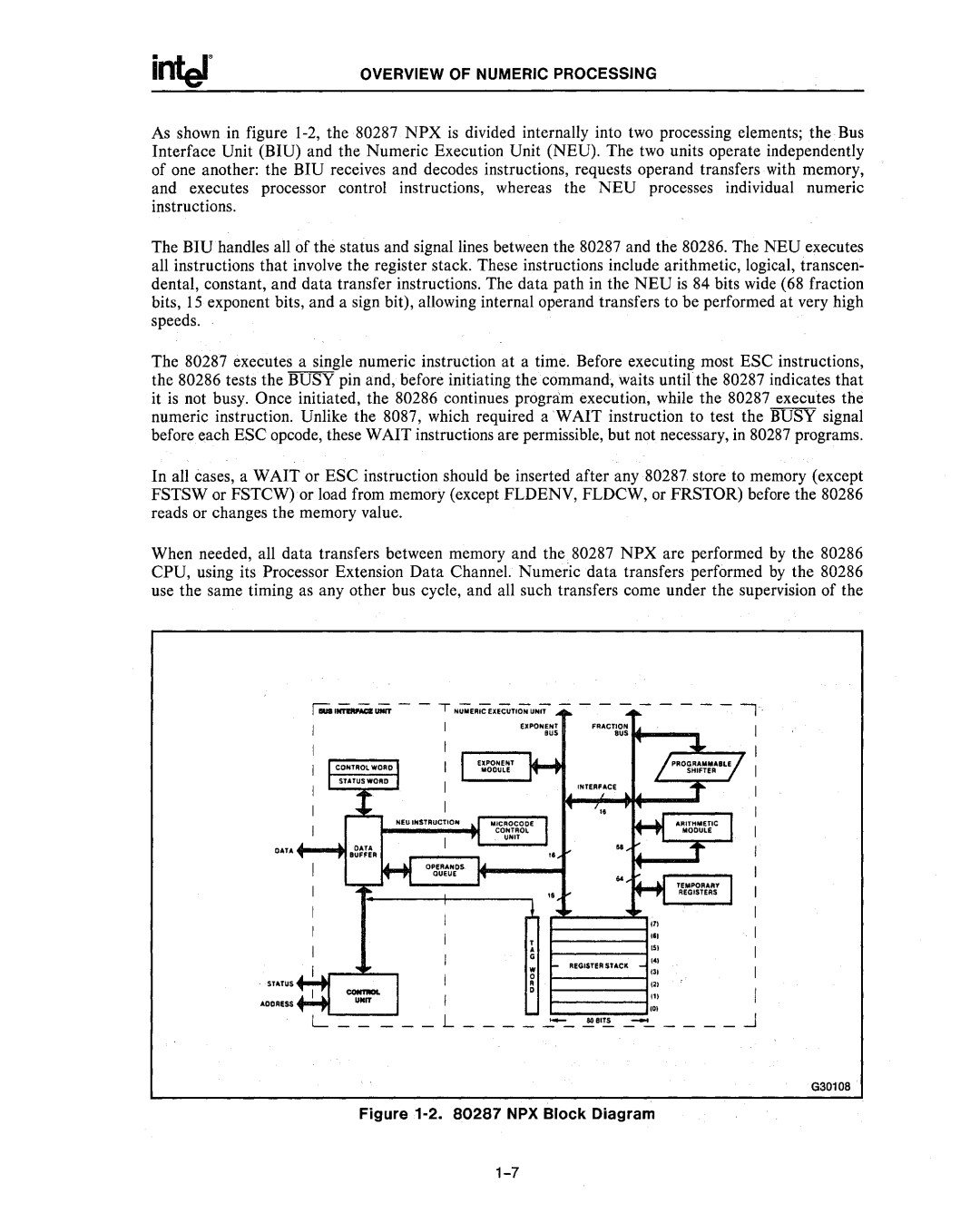
Overview of Numeric Processing
Page
Performance
Introduction to the 80287 Numeric Processor Extension
Fxam StackO assumed Examine
Overview of Numeric Processing
± Vb2 4ac
Applications
Upgradability
PASCAL-286 FORTRAN-286
Programming Interface
Numeric Data Types
Hardware Interface
~r=~=~
NPX Register Stack
Numeric Processor Architecture
80287 Register Set
NPX Status Word
Status Word
Control Word
Infinity, positive
Inter
Tag Word Format
Number System
Computation Fundamentals
Number System
Data Types and Formats
Data Formats
Binary Integers
Rounding Control
·6. Rounding Modes
Precision Control
Special Numeric Values
Special Computational Situations
Nonnormal Real Numbers
Overview of Numeric Processing
Denormalization Process
Unnormals-Descendents of Denormal Operands
FLD
Frndint
Fsqrt
FIST, FISTP, Fbstp
Infinity
Fsqrt
FLD, FBLD1 FILD2 FST,FSTP
Fbstp FIST, Fistp
Fprem
+co
Ftst
Frndint
Fxtract
�......1 ---- 15 bits-----l..~1
Largest
Smallest
Zero Smallest
U U
Zero
U U2
Bits
Normals
Class NaNs
16. Temporary Real Encodings Sign Biased Exponent
Significand·
Zero Divisor
16. Temporary Real Encodings Contd
Invalid Operation
Overview of Numeric Processing Denormalized Operand
17. Exception Conditions and Masked Responses
Masked response to overflow exception earlier
17. Exception Conditions and Masked Responses Contd
11. Arithmetic Example Using Infinity
Software Exception Handling
Programming Numeric Applications
Page
Numeric Operands
80287 NPX Instruction SET
Compatibility with the 8087 NPX
Data Transfer Instructions
FAD D destination, source
Programming Numeric Applications
Arithmetic Instructions
Arithmetic Instructions
Fdiv Azimuth
Fadd
Fsub
Fmulp
Fsubrp / /destination/source
Fprem
Condition Code Interpretation after Fprem
Condition Code Interpretation after Fcom
Programming Numeric Applications Fabs
Fcom / /source
Comparison Instructions
Fxam
Fcompp
STO 1r
Fptan
FYL2XP1
Fpatan
F2XM1
FYL2X
Constant Instructions
Processor Control Instructions
Finitifninit
Fstsw AX/FNSTSW AX
FSAVE/FRSTOR Memory Layout
Fstenvifldenv Memory Layout
Ffree destination
Instruction Execution Time
12. Key to Operand Types
Programming Numeric Applications
13. Execution Penalties
Instruction Length
·14. Instruction Set Reference Data
14. Instruction Set Reference Data Contd
Fdivr
Programming Numeric Applications Fdecstp
Fdiv
Fdivp
Ficom BP+4.PARMCOUNT
Ffree ST1
Fiadd DISTANCE..TRAVELLED Fiadd Pulsecount SI
Ficom TOOL.NPASSES
Fimul Bearing
Fidivr Frequency
Fild Standoff DI
Fild RESPONSE.COUNT
Fistp Correctedtime
Fist OBS.COUNTSI
Fist BP.FACTOREDPULSES
Fistp BX.ALPHACOUNT SI
FLDLG2
FLD Reading 81.PRE88URE
FLO 8AVEREADING
Fldcw Controlword
Floz
FLOL2E
FLOL2T
Flopi
Fpatan
Fmul Speedfactor
Fmulp ST1,ST
Fsave BP
·14. Instruction Set Reference Data Contd
Fptan
Frstor BP
Fstcw Savecontrol
FST ST3
FST Correlation
FST Meanreading
Fstp Regsave SI
Fstp BX.ADJUSTEDRPM
Fstp ST2
Fstp Totaldosage
Fsubrp ST1,ST
Fsubr ST,ST1
Fsubr Vectorsi
Fsubr BX.INDEX
FYL2XP1
Fxch ST2
FYL2X
High-Level Languages
Programming Facilities
15. PLlM-286 Built-In Procedures
Interpretation Data Types
ASM286
BIT String Shorti Nteger OFFFFFF82H HEX Must Start
Status Word Record Definition
TR E Q
Filo BP.BETA
17. Addressing Mode Examples
Fiaooalpha FOIVRALPHA.BETA
Fsub Alpha SI
Sample PL/M-286 Program
It *it
Concurrent Processing with
Emulation
·7. Sample ASM286 Program
Intel Programming Numeric Applications
Sample ASM286 Program Contd
Instruction Synchronization
Managing Concurrency
Data Synchronization
Synchronizing References to Shared Data
Error Synchronization
MOV
Fsgrt
System-Level Numeric Programming
Page
Processor Extension Data Channel
Real-Address Mode and Protected Virtual-Address Mode
Architecture
Recognizing. the 80287 NPX
Dedicated and Reserved 1/0 Locations
Processor Initialization and Control
System Initialization
Software Routine to Recognize
SYSTEM-LEVEL Numeric Programming
Configuring the Numerics Environment
NPX Processor State Following Initialization
Initializing
Handling Numeric Processing Exceptions
Inter
Simultaneous Exception Response
Precedence of NPX Exceptions
Numeric Programming Examples
Page
Chapter Numeric Programming Examples
XAM
Jump Table for Examine Routine
Conditional Branching for Fxam Contd
Numeric Programming Examples
Proc
MOV Byte PTR IBP-121, OH Fldenv
Fnsave BP-941
FLOATING-POINT to Ascii Conversion Examples
It116
Ebde
DoeF
\ii.t
4BB
Lei
Function. Partitioning
Description of Operation
Exception Considerations
Special Instructions
Scaling the Value
Trigonometric Calculation Examples
Output Format
Numeric Programming Examples
Calculating Trigonometric Functions
207
Arg
0o,3
Coce
4676
Page
Machine Instruction Encoding and Decoding
Page
REG
OP-A MOD OP-S Displacement Format OP-AMOD
Table A·2. Machine Instruction Decodin.9 Guide
Machine Instruction Encoding and Decoding
MOD10
Machine Instruction Encoding and Decoding
Modoo
MOD01
Table A-2. Machine Instruction Decoding Guide Contd
XXX
1REG
Oreg
Fstswax
Page
Appendix Compatibility Between NPX
Page
80287 NPX
Appendix B Compatibility Between
NI NIT
Appendixc·
Page
Appendix C Implementing the Ieee P754 Standard
Additional Software to Meet the Standard
Implementing the Ieee P754 Standard
Page
Glossary of 80287 and Floating-Point Terminology
Page
Glossary-1
Glossary FLOATING-POINT Terminology
Inter Glossary of 80287 and FLOATING-POINT Terminology
Glossary-3
Glossary of 80287 and FLOATING-POINT Terminology
Glossary-4
Glossary of 80287 and FLOATING-POINT Terminology
Page
Index
Index-2
NO-WAIT Form
Index-4
Inter
Inter
IntJ
European Sales Offices