Signal Description
2.10Voltage Pins
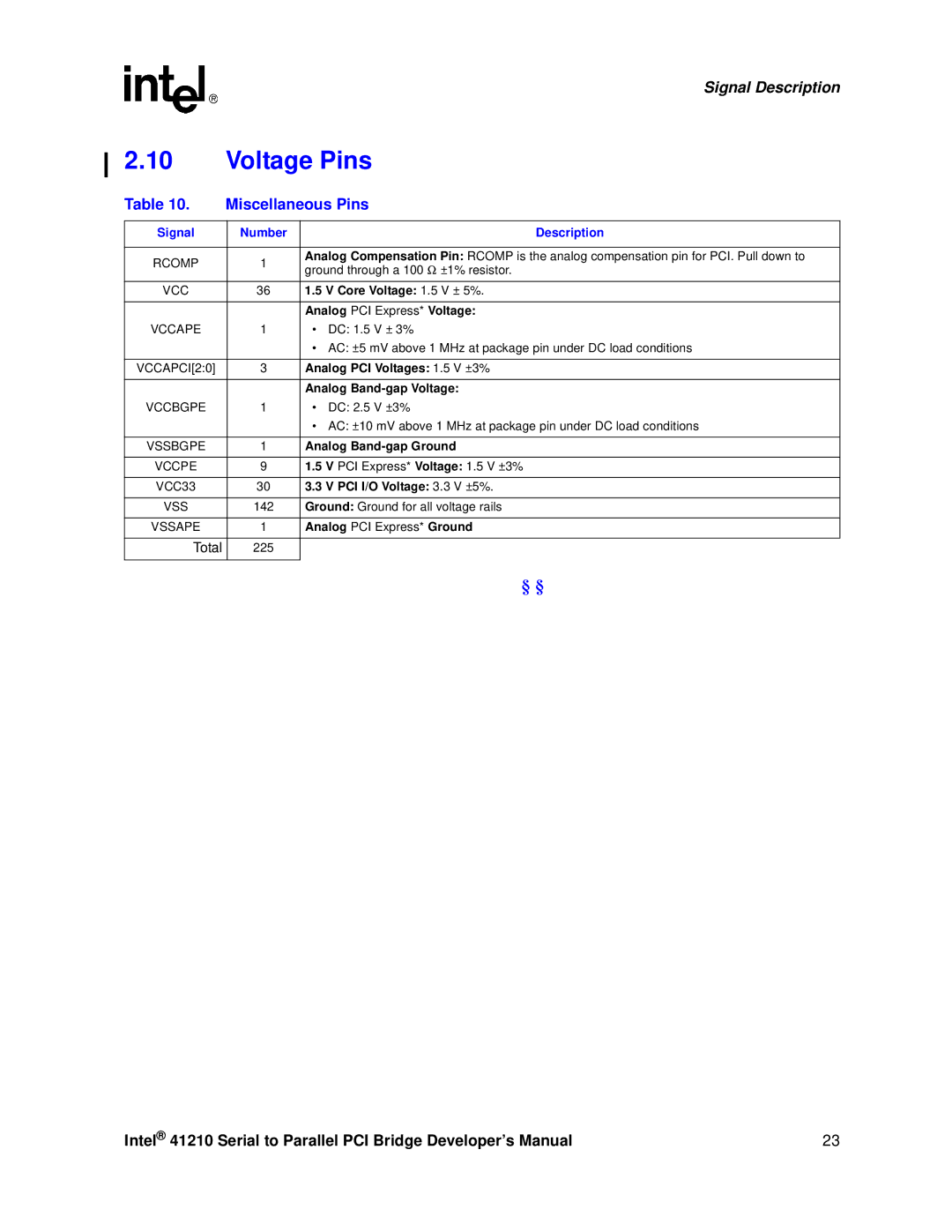
Table 10. | Miscellaneous Pins | ||
|
|
| |
Signal | Number | Description | |
|
|
| |
RCOMP | 1 | Analog Compensation Pin: RCOMP is the analog compensation pin for PCI. Pull down to | |
ground through a 100 Ω ±1% resistor. | |||
|
| ||
|
|
| |
VCC | 36 | 1.5 V Core Voltage: 1.5 V ± 5%. | |
|
|
| |
|
| Analog PCI Express* Voltage: | |
VCCAPE | 1 | • DC: 1.5 V ± 3% | |
|
| • AC: ±5 mV above 1 MHz at package pin under DC load conditions | |
|
|
| |
VCCAPCI[2:0] | 3 | Analog PCI Voltages: 1.5 V ±3% | |
|
|
| |
|
| Analog | |
VCCBGPE | 1 | • DC: 2.5 V ±3% | |
|
| • AC: ±10 mV above 1 MHz at package pin under DC load conditions | |
|
|
| |
VSSBGPE | 1 | Analog | |
|
|
| |
VCCPE | 9 | 1.5 V PCI Express* Voltage: 1.5 V ±3% | |
|
|
| |
VCC33 | 30 | 3.3 V PCI I/O Voltage: 3.3 V ±5%. | |
|
|
| |
VSS | 142 | Ground: Ground for all voltage rails | |
|
|
| |
VSSAPE | 1 | Analog PCI Express* Ground | |
|
|
| |
Total | 225 |
| |
|
|
| |
§ §
Intel® 41210 Serial to Parallel PCI Bridge Developer’s Manual | 23 |
