| Clock and Reset |
Clock and Reset | 10 |
|
|
10.1Clocking
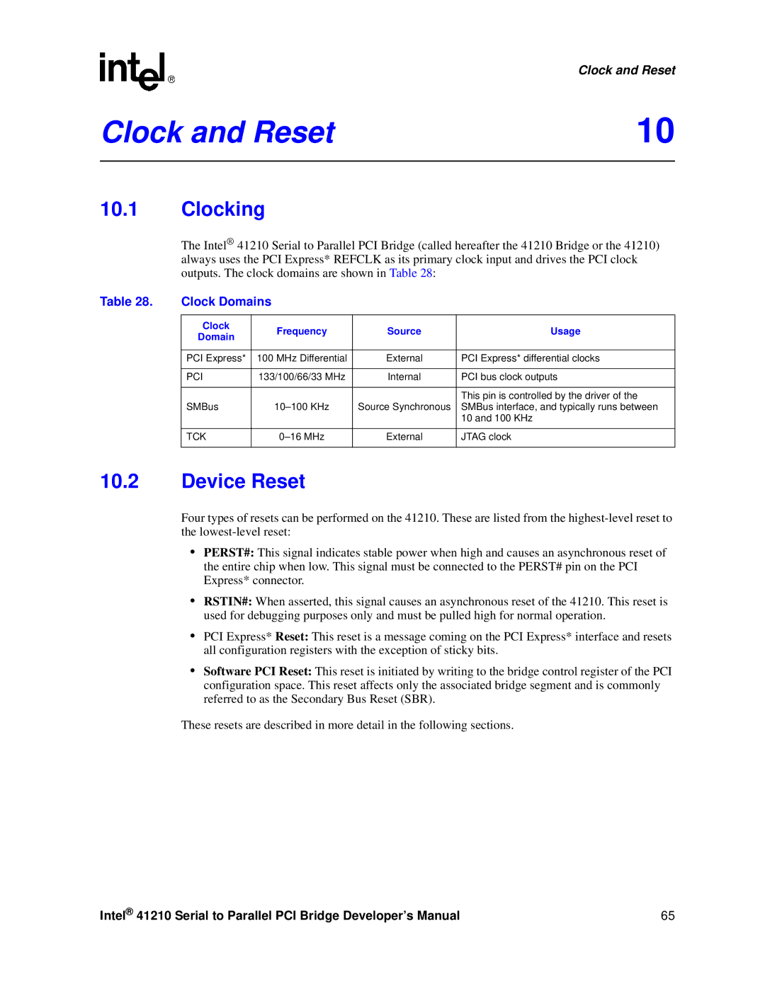
The Intel® 41210 Serial to Parallel PCI Bridge (called hereafter the 41210 Bridge or the 41210) always uses the PCI Express* REFCLK as its primary clock input and drives the PCI clock outputs. The clock domains are shown in Table 28:
Table 28. | Clock Domains |
|
| |
|
|
|
|
|
| Clock | Frequency | Source | Usage |
| Domain | |||
|
|
|
| |
|
|
|
|
|
| PCI Express* | 100 MHz Differential | External | PCI Express* differential clocks |
|
|
|
|
|
| PCI | 133/100/66/33 MHz | Internal | PCI bus clock outputs |
|
|
|
|
|
|
|
|
| This pin is controlled by the driver of the |
| SMBus | Source Synchronous | SMBus interface, and typically runs between | |
|
|
|
| 10 and 100 KHz |
|
|
|
|
|
| TCK | External | JTAG clock | |
|
|
|
|
|
10.2Device Reset
Four types of resets can be performed on the 41210. These are listed from the
•PERST#: This signal indicates stable power when high and causes an asynchronous reset of the entire chip when low. This signal must be connected to the PERST# pin on the PCI Express* connector.
•RSTIN#: When asserted, this signal causes an asynchronous reset of the 41210. This reset is used for debugging purposes only and must be pulled high for normal operation.
•PCI Express* Reset: This reset is a message coming on the PCI Express* interface and resets all configuration registers with the exception of sticky bits.
•Software PCI Reset: This reset is initiated by writing to the bridge control register of the PCI configuration space. This reset affects only the associated bridge segment and is commonly referred to as the Secondary Bus Reset (SBR).
These resets are described in more detail in the following sections.
Intel® 41210 Serial to Parallel PCI Bridge Developer’s Manual | 65 |