Signal Description
2.4PCI Bus Interface 64-Bit Extension (Two Interfaces)
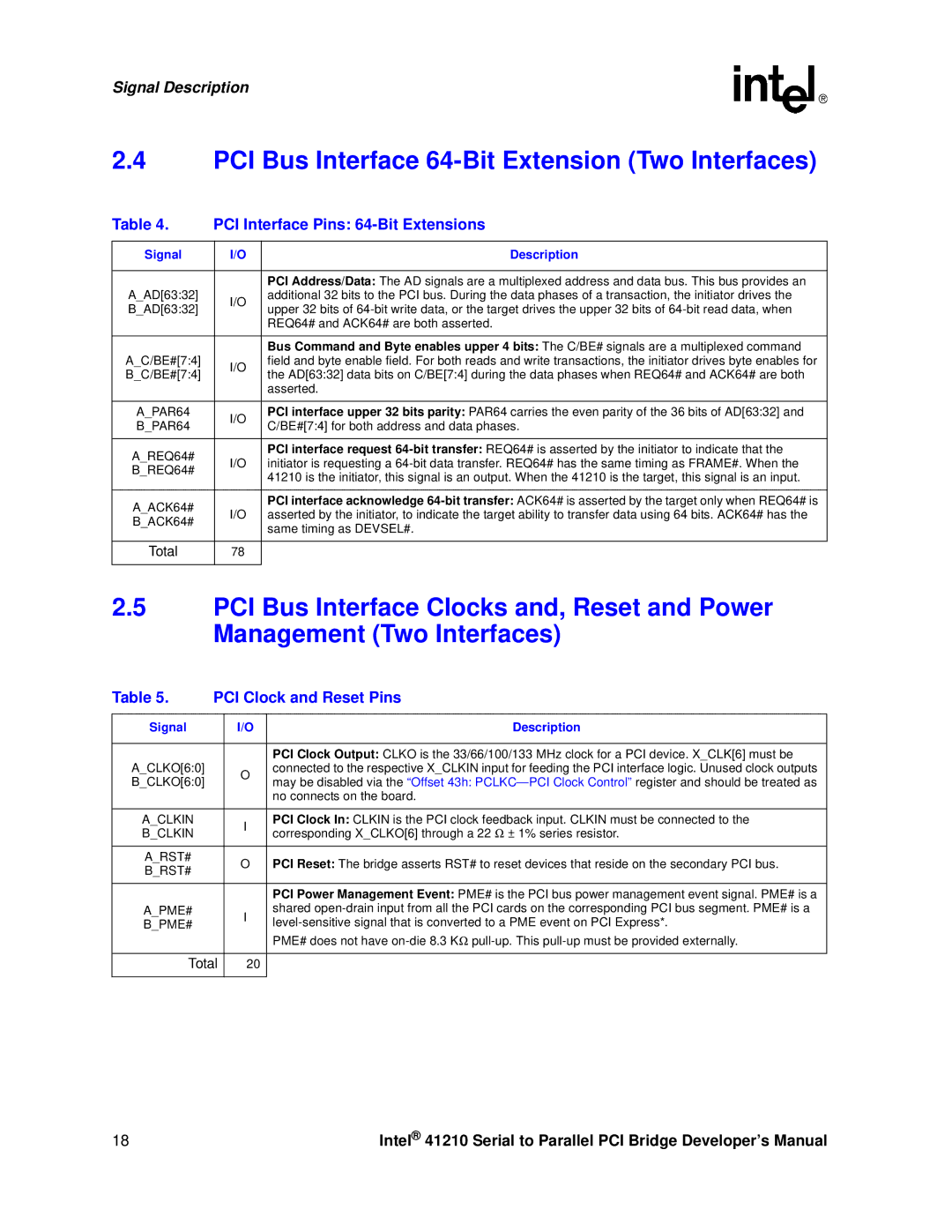
Table 4. | PCI Interface Pins: | ||
|
|
| |
Signal | I/O | Description | |
|
|
| |
|
| PCI Address/Data: The AD signals are a multiplexed address and data bus. This bus provides an | |
A_AD[63:32] | I/O | additional 32 bits to the PCI bus. During the data phases of a transaction, the initiator drives the | |
B_AD[63:32] | upper 32 bits of | ||
| |||
|
| REQ64# and ACK64# are both asserted. | |
|
|
| |
|
| Bus Command and Byte enables upper 4 bits: The C/BE# signals are a multiplexed command | |
A_C/BE#[7:4] | I/O | field and byte enable field. For both reads and write transactions, the initiator drives byte enables for | |
B_C/BE#[7:4] | the AD[63:32] data bits on C/BE[7:4] during the data phases when REQ64# and ACK64# are both | ||
| |||
|
| asserted. | |
|
|
| |
A_PAR64 | I/O | PCI interface upper 32 bits parity: PAR64 carries the even parity of the 36 bits of AD[63:32] and | |
B_PAR64 | C/BE#[7:4] for both address and data phases. | ||
| |||
|
|
| |
A_REQ64# |
| PCI interface request | |
I/O | initiator is requesting a | ||
B_REQ64# | |||
| 41210 is the initiator, this signal is an output. When the 41210 is the target, this signal is an input. | ||
|
| ||
|
|
| |
A_ACK64# |
| PCI interface acknowledge | |
I/O | asserted by the initiator, to indicate the target ability to transfer data using 64 bits. ACK64# has the | ||
B_ACK64# | |||
| same timing as DEVSEL#. | ||
|
| ||
|
|
| |
Total | 78 |
| |
|
|
| |
2.5PCI Bus Interface Clocks and, Reset and Power Management (Two Interfaces)
Table 5. | PCI Clock and Reset Pins |
| ||
|
|
|
|
|
Signal |
| I/O |
| Description |
|
|
|
| |
A_CLKO[6:0] |
|
| PCI Clock Output: CLKO is the 33/66/100/133 MHz clock for a PCI device. X_CLK[6] must be | |
| O | connected to the respective X_CLKIN input for feeding the PCI interface logic. Unused clock outputs | ||
B_CLKO[6:0] |
| may be disabled via the “Offset 43h: | ||
|
| |||
|
|
| no connects on the board. |
|
|
|
|
| |
A_CLKIN |
| I | PCI Clock In: CLKIN is the PCI clock feedback input. CLKIN must be connected to the | |
B_CLKIN |
| corresponding X_CLKO[6] through a 22 Ω | ± 1% series resistor. | |
|
| |||
|
|
|
|
|
A_RST# |
| O | PCI Reset: The bridge asserts RST# to reset devices that reside on the secondary PCI bus. | |
B_RST# |
| |||
|
|
|
| |
|
|
|
| |
|
|
| PCI Power Management Event: PME# is the PCI bus power management event signal. PME# is a | |
A_PME# |
| I | shared | |
B_PME# |
| |||
|
| |||
|
|
| PME# does not have | |
|
|
|
| |
Total | 20 |
|
| |
|
|
|
|
|
18 | Intel® 41210 Serial to Parallel PCI Bridge Developer’s Manual |