Register Description
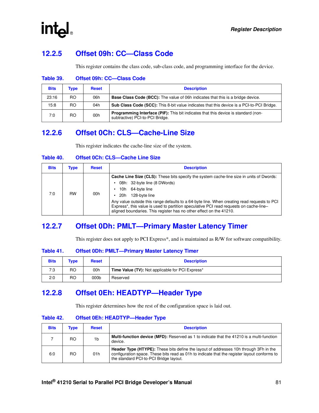
12.2.5Offset 09h: CC—Class Code
This register contains the class code,
Table 39. | Offset 09h: | |||
|
|
|
|
|
Bits |
| Type | Reset | Description |
|
|
|
|
|
23:16 |
| RO | 06h | Base Class Code (BCC): The value of 06h indicates that this is a bridge device. |
|
|
|
|
|
15:8 |
| RO | 04h | Sub Class Code (SCC): This |
|
|
|
|
|
7:0 |
| RO | 00h | Programming Interface (PIF): This bit indicates that this device is standard (non- |
| subtractive) | |||
|
|
|
| |
|
|
|
|
|
12.2.6Offset 0Ch: CLS—Cache-Line Size
This register indicates the
Table 40. | Offset 0Ch: | |||||
|
|
|
|
|
|
|
Bits |
| Type | Reset |
|
| Description |
|
|
|
|
| ||
|
|
|
| Cache Line Size (CLS): These bits specify the system | ||
|
|
|
| • | 08h: |
|
7:0 |
| RW | 00h | • | 10h | |
| • | 20h | ||||
|
|
|
| |||
|
|
|
| Any value outside this range defaults to a | ||
|
|
|
| Express*, this value is used to partition speculative PCI read requests on | ||
|
|
|
| aligned boundaries. This register has no other effect on the 41210. | ||
|
|
|
|
|
|
|
12.2.7Offset 0Dh: PMLT—Primary Master Latency Timer
This register does not apply to PCI Express*, and is maintained as R/W for software compatibility.
Table 41. | Offset 0Dh: | |||
|
|
|
|
|
Bits |
| Type | Reset | Description |
|
|
|
|
|
7:3 |
| RO | 00h | Time Value (TV): Not applicable for PCI Express* |
|
|
|
|
|
2:0 |
| RO | 000b | Reserved |
|
|
|
|
|
12.2.8Offset 0Eh: HEADTYP—Header Type
This register determines how the rest of the configuration space is laid out.
Table 42. | Offset 0Eh: | |||
|
|
|
|
|
Bits |
| Type | Reset | Description |
|
|
|
|
|
7 |
| RO | 1b | |
| device. | |||
|
|
|
| |
|
|
|
|
|
|
|
|
| Header Type (HTYPE): These bits define the layout of addresses 10h through 3Fh in the |
6:0 |
| RO | 01h | configuration space. These bits read as 01h to indicate that the register layout conforms to |
|
|
|
| the standard |
|
|
|
|
|
Intel® 41210 Serial to Parallel PCI Bridge Developer’s Manual | 81 |
