|
|
|
|
|
| Register Description | |
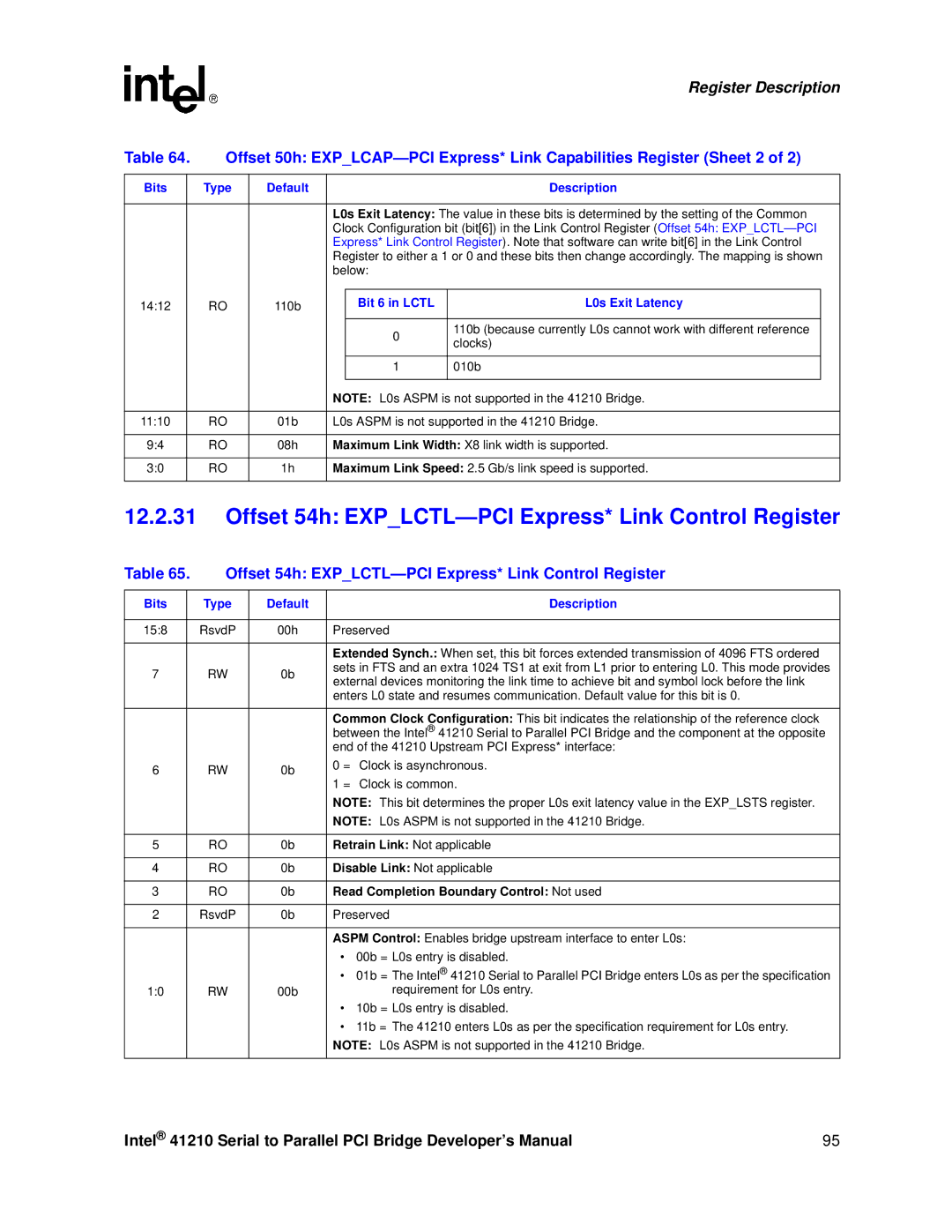
Table 64. | Offset 50h: | ||||||
|
|
|
|
|
|
|
|
Bits |
| Type | Default |
|
| Description | |
|
|
|
|
|
|
|
|
|
|
|
| L0s Exit Latency: The value in these bits is determined by the setting of the Common | |||
|
|
|
| Clock Configuration bit (bit[6]) in the Link Control Register (Offset 54h: | |||
|
|
|
| Express* Link Control Register). Note that software can write bit[6] in the Link Control | |||
|
|
|
| Register to either a 1 or 0 and these bits then change accordingly. The mapping is shown | |||
|
|
|
| below: |
|
| |
|
|
|
|
|
|
|
|
14:12 |
| RO | 110b |
| Bit 6 in LCTL | L0s Exit Latency |
|
|
|
|
|
|
|
|
|
|
|
|
|
| 0 | 110b (because currently L0s cannot work with different reference |
|
|
|
|
|
| clocks) |
| |
|
|
|
|
|
|
| |
|
|
|
|
|
|
|
|
|
|
|
|
| 1 | 010b |
|
|
|
|
|
|
|
|
|
|
|
|
| NOTE: L0s ASPM is not supported in the 41210 Bridge. | |||
|
|
|
|
|
|
|
|
11:10 |
| RO | 01b | L0s ASPM is not supported in the 41210 Bridge. | |||
|
|
|
|
|
|
|
|
9:4 |
| RO | 08h | Maximum Link Width: X8 link width is supported. | |||
|
|
|
|
|
|
|
|
3:0 |
| RO | 1h | Maximum Link Speed: 2.5 Gb/s link speed is supported. | |||
|
|
|
|
|
|
|
|
12.2.31Offset 54h: EXP_LCTL—PCI Express* Link Control Register
Table 65. | Offset 54h: | ||||
|
|
|
|
|
|
Bits |
| Type | Default |
| Description |
|
|
|
|
| |
15:8 |
| RsvdP | 00h | Preserved | |
|
|
|
|
| |
|
|
|
| Extended Synch.: When set, this bit forces extended transmission of 4096 FTS ordered | |
7 |
| RW | 0b | sets in FTS and an extra 1024 TS1 at exit from L1 prior to entering L0. This mode provides | |
| external devices monitoring the link time to achieve bit and symbol lock before the link | ||||
|
|
|
| ||
|
|
|
| enters L0 state and resumes communication. Default value for this bit is 0. | |
|
|
|
|
| |
|
|
|
| Common Clock Configuration: This bit indicates the relationship of the reference clock | |
|
|
|
| between the Intel® 41210 Serial to Parallel PCI Bridge and the component at the opposite | |
|
|
|
| end of the 41210 Upstream PCI Express* interface: | |
6 |
| RW | 0b | 0 = Clock is asynchronous. | |
| 1 = Clock is common. | ||||
|
|
|
| ||
|
|
|
| NOTE: This bit determines the proper L0s exit latency value in the EXP_LSTS register. | |
|
|
|
| NOTE: L0s ASPM is not supported in the 41210 Bridge. | |
|
|
|
|
| |
5 |
| RO | 0b | Retrain Link: Not applicable | |
|
|
|
|
| |
4 |
| RO | 0b | Disable Link: Not applicable | |
|
|
|
|
| |
3 |
| RO | 0b | Read Completion Boundary Control: Not used | |
|
|
|
|
| |
2 |
| RsvdP | 0b | Preserved | |
|
|
|
|
| |
|
|
|
| ASPM Control: Enables bridge upstream interface to enter L0s: | |
|
|
|
| • | 00b = L0s entry is disabled. |
|
|
|
| • 01b = The Intel® 41210 Serial to Parallel PCI Bridge enters L0s as per the specification | |
1:0 |
| RW | 00b |
| requirement for L0s entry. |
|
|
|
| • | 10b = L0s entry is disabled. |
|
|
|
| • | 11b = The 41210 enters L0s as per the specification requirement for L0s entry. |
|
|
|
| NOTE: L0s ASPM is not supported in the 41210 Bridge. | |
|
|
|
|
|
|
Intel® 41210 Serial to Parallel PCI Bridge Developer’s Manual | 95 |