Register Description
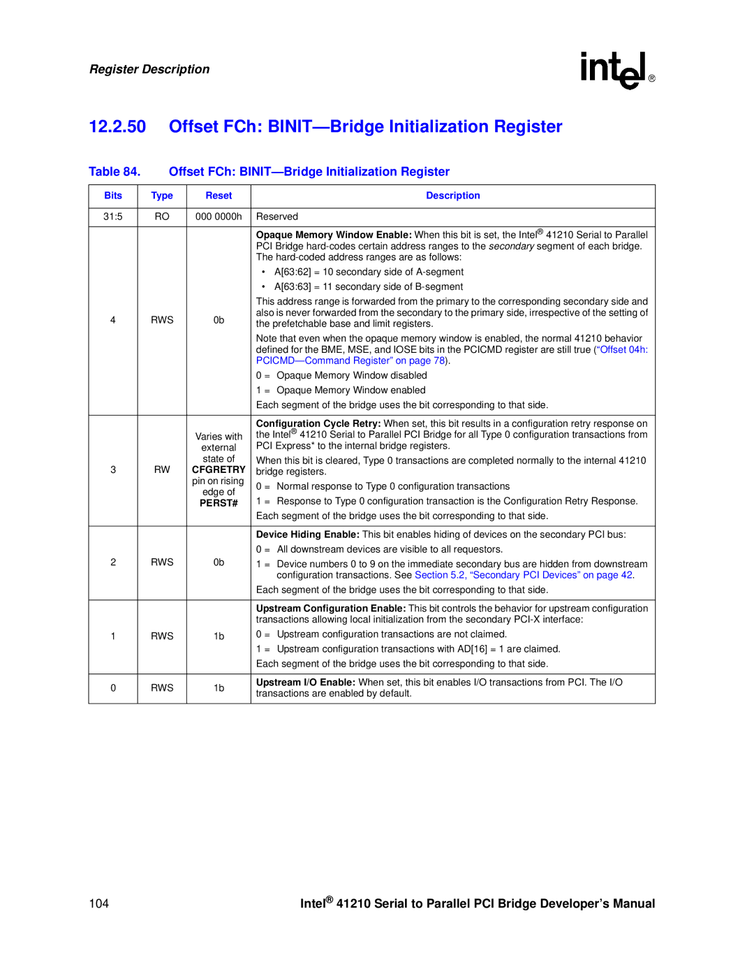
12.2.50Offset FCh: BINIT—Bridge Initialization Register
Table 84. | Offset FCh: | |||
|
|
|
|
|
Bits |
| Type | Reset | Description |
|
|
|
|
|
31:5 |
| RO | 000 0000h | Reserved |
|
|
|
|
|
|
|
|
| Opaque Memory Window Enable: When this bit is set, the Intel® 41210 Serial to Parallel |
|
|
|
| PCI Bridge |
|
|
|
| The |
|
|
|
| • A[63:62] = 10 secondary side of |
|
|
|
| • A[63:63] = 11 secondary side of |
|
|
|
| This address range is forwarded from the primary to the corresponding secondary side and |
4 |
| RWS | 0b | also is never forwarded from the secondary to the primary side, irrespective of the setting of |
| the prefetchable base and limit registers. | |||
|
|
|
| |
|
|
|
| Note that even when the opaque memory window is enabled, the normal 41210 behavior |
|
|
|
| defined for the BME, MSE, and IOSE bits in the PCICMD register are still true (“Offset 04h: |
|
|
|
|
|
|
|
|
| 0 = Opaque Memory Window disabled |
|
|
|
| 1 = Opaque Memory Window enabled |
|
|
|
| Each segment of the bridge uses the bit corresponding to that side. |
|
|
|
|
|
|
|
|
| Configuration Cycle Retry: When set, this bit results in a configuration retry response on |
|
|
| Varies with | the Intel® 41210 Serial to Parallel PCI Bridge for all Type 0 configuration transactions from |
|
|
| external | PCI Express* to the internal bridge registers. |
3 |
| RW | state of | When this bit is cleared, Type 0 transactions are completed normally to the internal 41210 |
| CFGRETRY | bridge registers. | ||
|
|
| pin on rising | 0 = Normal response to Type 0 configuration transactions |
|
|
| edge of | |
|
|
| 1 = Response to Type 0 configuration transaction is the Configuration Retry Response. | |
|
|
| PERST# | |
|
|
|
| Each segment of the bridge uses the bit corresponding to that side. |
|
|
|
|
|
|
|
|
| Device Hiding Enable: This bit enables hiding of devices on the secondary PCI bus: |
|
|
|
| 0 = All downstream devices are visible to all requestors. |
2 |
| RWS | 0b | 1 = Device numbers 0 to 9 on the immediate secondary bus are hidden from downstream |
|
|
|
| configuration transactions. See Section 5.2, “Secondary PCI Devices” on page 42. |
|
|
|
| Each segment of the bridge uses the bit corresponding to that side. |
|
|
|
|
|
|
|
|
| Upstream Configuration Enable: This bit controls the behavior for upstream configuration |
|
|
|
| transactions allowing local initialization from the secondary |
1 |
| RWS | 1b | 0 = Upstream configuration transactions are not claimed. |
|
|
|
| 1 = Upstream configuration transactions with AD[16] = 1 are claimed. |
|
|
|
| Each segment of the bridge uses the bit corresponding to that side. |
|
|
|
|
|
0 |
| RWS | 1b | Upstream I/O Enable: When set, this bit enables I/O transactions from PCI. The I/O |
| transactions are enabled by default. | |||
|
|
|
| |
|
|
|
|
|
104 | Intel® 41210 Serial to Parallel PCI Bridge Developer’s Manual |
