Register Description
12.2.1Offset 00h: ID—Identifiers
|
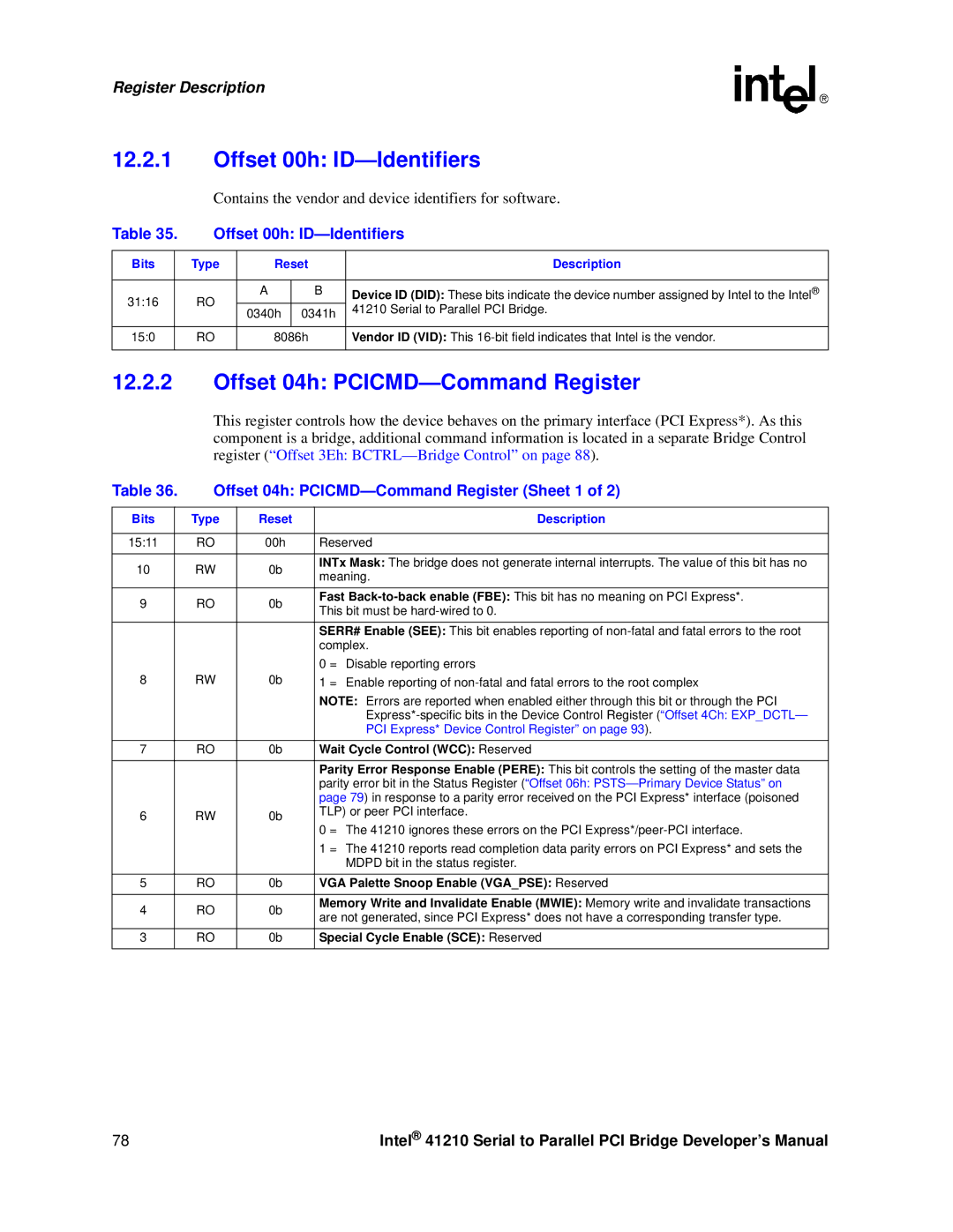
| Contains the vendor and device identifiers for software. | ||||
Table 35. | Offset 00h: | |||||
|
|
|
|
|
|
|
Bits |
| Type |
| Reset | Description | |
|
|
|
|
|
|
|
31:16 |
| RO | A |
| B | Device ID (DID): These bits indicate the device number assigned by Intel to the Intel® |
| 0340h | 0341h | 41210 Serial to Parallel PCI Bridge. | |||
|
|
| ||||
|
|
|
| |||
|
|
|
|
|
|
|
15:0 |
| RO |
| 8086h | Vendor ID (VID): This | |
|
|
|
|
|
|
|
12.2.2Offset 04h: PCICMD—Command Register
This register controls how the device behaves on the primary interface (PCI Express*). As this component is a bridge, additional command information is located in a separate Bridge Control register (“Offset 3Eh:
Table 36. | Offset 04h: | |||
|
|
|
|
|
Bits |
| Type | Reset | Description |
|
|
|
|
|
15:11 |
| RO | 00h | Reserved |
|
|
|
|
|
10 |
| RW | 0b | INTx Mask: The bridge does not generate internal interrupts. The value of this bit has no |
| meaning. | |||
|
|
|
| |
9 |
| RO | 0b | Fast |
| This bit must be | |||
|
|
|
| |
|
|
|
| SERR# Enable (SEE): This bit enables reporting of |
|
|
|
| complex. |
8 |
| RW | 0b | 0 = Disable reporting errors |
| 1 = Enable reporting of | |||
|
|
|
| NOTE: Errors are reported when enabled either through this bit or through the PCI |
|
|
|
| |
|
|
|
| PCI Express* Device Control Register” on page 93). |
7 |
| RO | 0b | Wait Cycle Control (WCC): Reserved |
|
|
|
|
|
|
|
|
| Parity Error Response Enable (PERE): This bit controls the setting of the master data |
|
|
|
| parity error bit in the Status Register (“Offset 06h: |
|
|
|
| page 79) in response to a parity error received on the PCI Express* interface (poisoned |
6 |
| RW | 0b | TLP) or peer PCI interface. |
| 0 = The 41210 ignores these errors on the PCI | |||
|
|
|
| |
|
|
|
| 1 = The 41210 reports read completion data parity errors on PCI Express* and sets the |
|
|
|
| MDPD bit in the status register. |
|
|
|
|
|
5 |
| RO | 0b | VGA Palette Snoop Enable (VGA_PSE): Reserved |
|
|
|
|
|
4 |
| RO | 0b | Memory Write and Invalidate Enable (MWIE): Memory write and invalidate transactions |
| are not generated, since PCI Express* does not have a corresponding transfer type. | |||
|
|
|
| |
3 |
| RO | 0b | Special Cycle Enable (SCE): Reserved |
|
|
|
|
|
78 | Intel® 41210 Serial to Parallel PCI Bridge Developer’s Manual |