Addressing
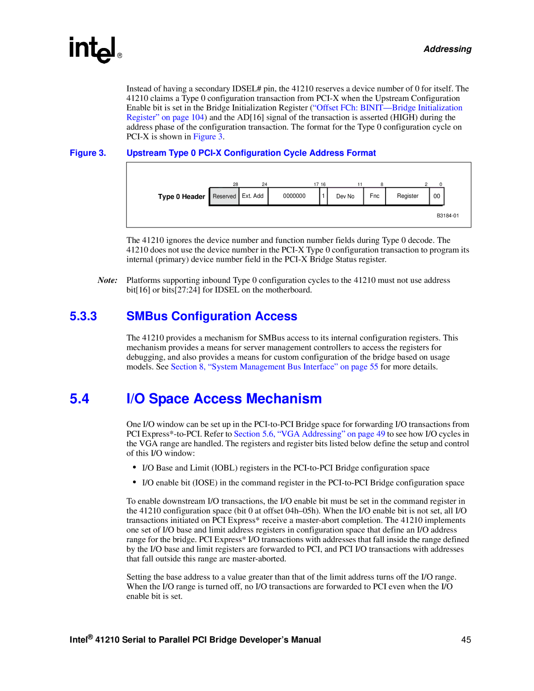
Instead of having a secondary IDSEL# pin, the 41210 reserves a device number of 0 for itself. The 41210 claims a Type 0 configuration transaction from
Figure 3. Upstream Type 0 PCI-X Configuration Cycle Address Format
Type 0 Header
31 30 29 28 27 26 | 25 24 23 22 21 20 | 19 | 18 17 16 15 14 13 | 12 11 10 | 9 | 8 | 7 | 6 | 5 | 4 | 3 | 2 | 1 | 0 |
| |||||
Reserved | Ext. Add | 0000000 |
| 1 | Dev No | Fnc |
|
| Register |
| 00 |
| ||||||||
|
|
|
|
|
|
|
|
|
|
|
|
|
|
|
|
|
|
|
|
|
The 41210 ignores the device number and function number fields during Type 0 decode. The 41210 does not use the device number in the
Note: Platforms supporting inbound Type 0 configuration cycles to the 41210 must not use address bit[16] or bits[27:24] for IDSEL on the motherboard.
5.3.3SMBus Configuration Access
The 41210 provides a mechanism for SMBus access to its internal configuration registers. This mechanism provides a means for server management controllers to access the registers for debugging, and also provides a means for custom configuration of the bridge based on usage models. See Section 8, “System Management Bus Interface” on page 55 for more details.
5.4I/O Space Access Mechanism
One I/O window can be set up in the
•I/O Base and Limit (IOBL) registers in the
•I/O enable bit (IOSE) in the command register in the
To enable downstream I/O transactions, the I/O enable bit must be set in the command register in the 41210 configuration space (bit 0 at offset
Setting the base address to a value greater than that of the limit address turns off the I/O range. When the I/O range is turned off, no I/O transactions are forwarded to PCI even when the I/O enable bit is set.
Intel® 41210 Serial to Parallel PCI Bridge Developer’s Manual | 45 |