Register Description
12.2.12Offset 1Eh: SSTS—Secondary Status
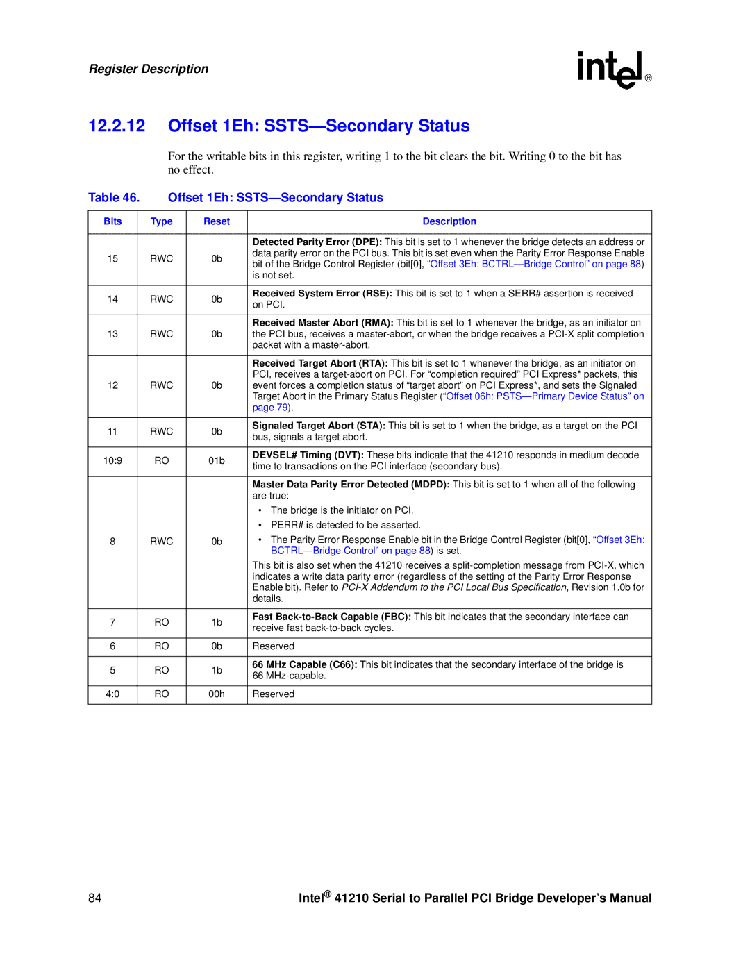
For the writable bits in this register, writing 1 to the bit clears the bit. Writing 0 to the bit has no effect.
Table 46. | Offset 1Eh: | |||
|
|
|
|
|
Bits |
| Type | Reset | Description |
|
|
|
|
|
|
|
|
| Detected Parity Error (DPE): This bit is set to 1 whenever the bridge detects an address or |
15 |
| RWC | 0b | data parity error on the PCI bus. This bit is set even when the Parity Error Response Enable |
| bit of the Bridge Control Register (bit[0], “Offset 3Eh: | |||
|
|
|
| |
|
|
|
| is not set. |
|
|
|
|
|
14 |
| RWC | 0b | Received System Error (RSE): This bit is set to 1 when a SERR# assertion is received |
| on PCI. | |||
|
|
|
| |
|
|
|
|
|
|
|
|
| Received Master Abort (RMA): This bit is set to 1 whenever the bridge, as an initiator on |
13 |
| RWC | 0b | the PCI bus, receives a |
|
|
|
| packet with a |
|
|
|
|
|
|
|
|
| Received Target Abort (RTA): This bit is set to 1 whenever the bridge, as an initiator on |
|
|
|
| PCI, receives a |
12 |
| RWC | 0b | event forces a completion status of “target abort” on PCI Express*, and sets the Signaled |
|
|
|
| Target Abort in the Primary Status Register (“Offset 06h: |
|
|
|
| page 79). |
|
|
|
|
|
11 |
| RWC | 0b | Signaled Target Abort (STA): This bit is set to 1 when the bridge, as a target on the PCI |
| bus, signals a target abort. | |||
|
|
|
| |
|
|
|
|
|
10:9 |
| RO | 01b | DEVSEL# Timing (DVT): These bits indicate that the 41210 responds in medium decode |
| time to transactions on the PCI interface (secondary bus). | |||
|
|
|
| |
|
|
|
|
|
|
|
|
| Master Data Parity Error Detected (MDPD): This bit is set to 1 when all of the following |
|
|
|
| are true: |
|
|
|
| • The bridge is the initiator on PCI. |
|
|
|
| • PERR# is detected to be asserted. |
8 |
| RWC | 0b | • The Parity Error Response Enable bit in the Bridge Control Register (bit[0], “Offset 3Eh: |
|
|
|
|
|
|
|
|
| This bit is also set when the 41210 receives a |
|
|
|
| indicates a write data parity error (regardless of the setting of the Parity Error Response |
|
|
|
| Enable bit). Refer to |
|
|
|
| details. |
|
|
|
|
|
7 |
| RO | 1b | Fast |
| receive fast | |||
|
|
|
| |
|
|
|
|
|
6 |
| RO | 0b | Reserved |
|
|
|
|
|
5 |
| RO | 1b | 66 MHz Capable (C66): This bit indicates that the secondary interface of the bridge is |
| 66 | |||
|
|
|
| |
|
|
|
|
|
4:0 |
| RO | 00h | Reserved |
|
|
|
|
|
84 | Intel® 41210 Serial to Parallel PCI Bridge Developer’s Manual |