Addressing

The base register consists of an 8-bit field at configuration address 1Ch, and a 16-bit field at address 30h. The top four bits (bits[7:4] of address 1Ch) of the 8-bit field define bits[15:12] of the I/O base address. The bottom four bits (bits[3:0]) read only as 0h to indicate that the 41210 supports 16-bit I/O addressing only. Bits[11:0] of the base address are assumed to be 0, which naturally aligns the base address to a 4 KB boundary. The I/O base upper 16-bit register at offset 30H is reserved. After chip reset, the value of the I/O base address is initialized to 0000H.

The I/O limit register consists of an 8-bit field at offset 1Dh and a 16-bit field at offset 32h. The top four bits (bits[7:4] of address 1Dh) of the 8-bit field define bits[15:12] of the I/O limit address. The bottom four bits (bits[3:0]) read only as 0h to indicate that 16-bit I/O addressing is supported.

Bits[11:0] of the limit address are assumed to be FFFh, which naturally aligns the limit address to the top of a 4 KB I/O address block. The 16 bits I/O base and limit registers at offsets 30h and 32h are not implemented, since the 41210 supports only 16-bit I/O addressing. After chip reset, the value of the I/O limit address is reset to 0FFFh (in other words, the lower 4 K in the 64 K space).

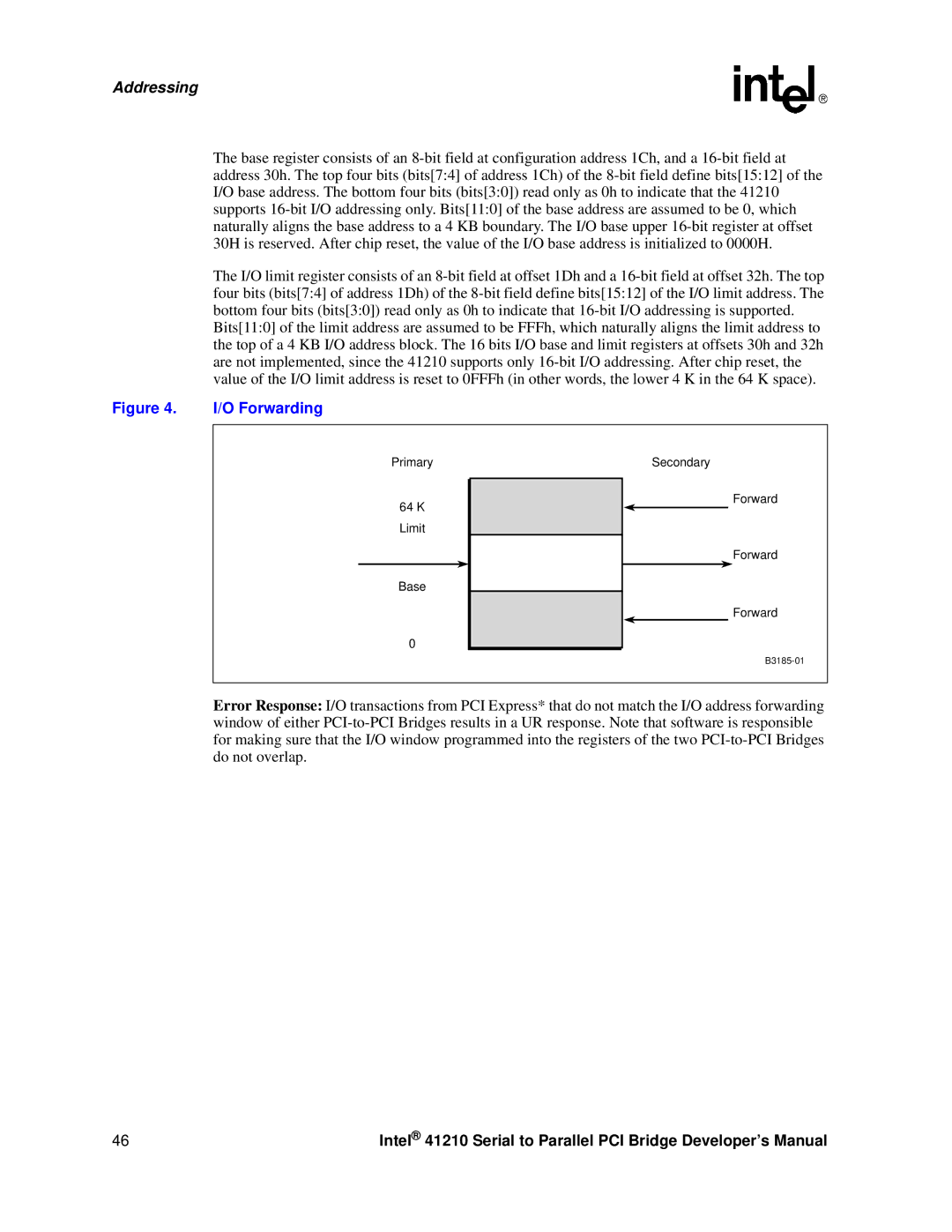
Figure 4. I/O Forwarding

Primary

64K Limit

Base

0

Secondary

Forward

Forward

Forward

B3185-01

Error Response: I/O transactions from PCI Express* that do not match the I/O address forwarding window of either PCI-to-PCI Bridges results in a UR response. Note that software is responsible for making sure that the I/O window programmed into the registers of the two PCI-to-PCI Bridges do not overlap.

46

Intel® 41210 Serial to Parallel PCI Bridge Developer’s Manual

Page 46
Image 46
Intel 41210 manual O Forwarding