80C186XL/80C188XL Microprocessor User’s Manual
80C186XL/80C188XL Microprocessor User’s Manual
Intel Corporation
Contents
Contents
Clock Generation
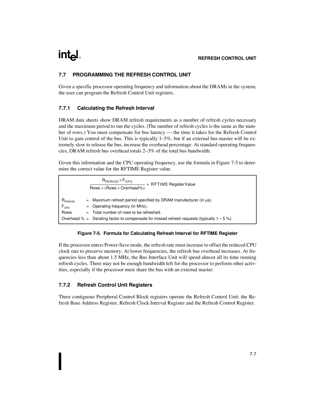
Setting the PCB Base Location
Power Management
LCS
Chapter Refresh Control Unit
Functional Overview Programming the TIMER/COUNTER Unit
Programming the Interrupt Control Unit
Functional Overview
Chapter Math Coprocessing
Chapter Once Mode
Figures
Reset Configuration
UCS
Interrupt Control Register for Noncascadable External Pins
10-9
Tables
Flag Bit Functions
Examples
Example
Introduction
Page
Chapter Introduction
HOW to USE this Manual
Feature 80C186XL 80C186EA 80C186EB 80C186EC
Comparison of 80C186 Modular Core Family Products
Related Documents
Related Documents and Software
Document/Software Title Order No
FaxBack Service
Electronic Support Systems
Bulletin Board System BBS
CompuServe Forums
World Wide Web
Technical Support
Product Literature
Training Classes
Page
Overview 80C186 Family Architecture
Page
Chapter Overview of the 80C186 Family Architecture
Architectural Overview
Simplified Functional Block Diagram of the 80C186 Family CPU
Execution Unit
Bus Interface Unit
Physical Address Generation
General Registers
General Registers
Segment Registers
Implicit Use of General Registers
Operations
Instruction Pointer
Segment Registers
Flags
Memory Segmentation
PSW Flags
Register Name
Register Mnemonic
Register Function
Logical Addresses
Segment Locations in Physical Memory
Data DS Code CS Stack SS Extra ES
Fffffh
2BFH 2BEH 2BDH 2BCH 2BBH 2BAH
Type of Memory Reference Default Alternate Offset
Dynamically Relocatable Code
Logical Address Sources
Before After Relocation Code Segment
Segment Code Data
Segment Data Extra
Stack Implementation
Reserved Memory and I/O Space
10. Stack Operation
Software Overview
Instruction Set
Data Transfer Instructions
General-Purpose
Input/Output
Pushf Popf U U O D I T S Z U a U P U C
Lahf S Z U a U P U C
Sahf 7 6 5 4 3 2 1
15 14 13 12 11 10 9 8 7 6 5 4 3 2 1
Multiplication
Addition
Subtraction
Division
Hex Bit Pattern Unsigned Signed Unpacked Packed Binary
Arithmetic Interpretation of 8-Bit Numbers
Bit Manipulation Instructions
Shifts
String Instructions
String Instruction Register and Flag Use
Program Transfer Instructions
CX AL/AX
Overview of the 80C186 Family Architecture
Iteration Control
Conditional Transfers
Unconditional Transfers
Interrupts
10. Interpretation of Conditional Transfers
Mnemonic Condition Tested Jump if…
11. Processor Control Instructions
Addressing Modes
Processor Control Instructions
Register and Immediate Operand Addressing Modes
Memory Addressing Modes
0000 Physical Addr
BIU
Opcode Mod R/M Displacement
13. Direct Addressing
14. Register Indirect Addressing
15. Based Addressing
Base Register
Displacement High Address Rate Age
Rate Base Vac
Register Dept Div Employee Age
18. Accessing an Array with Indexed Addressing
17. Indexed Addressing
19. Based Index Addressing
20. Accessing a Stacked Array with Based Index Addressing
Opcode Source EA Destination EA
Type Description
Data Types Used in the 80C186 Modular Core Family
12. Supported Data Types
BCD
23 C186 Modular Core Family Supported Data Types
Interrupts and Exception Handling
Interrupt/Exception Processing
3FE
3FC
Overview of the 80C186 Family Architecture
PSW
Interrupt Enable Bit
Stack
Trap Flag
Maskable Interrupts
Exceptions
Invalid Opcode Type
Software Interrupts
Interrupt Latency
Total
Interrupt Response Time
Clocks
Interrupt and Exception Priority
Execute Divide Service Routine
NMI
Iret
Trap Flag = ???
29. Simultaneous NMI and Single Step Interrupts
Interrupt Enable Bit IE = Trap Flag TF =
30. Simultaneous NMI, Single Step and Maskable Interrupt
Page
Bus Interface Unit
Page
Multiplexed Address and Data BUS
Address and Data BUS Concepts
1 16-Bit Data Bus
Fffff Ffffe Ffffd Ffffc
Physical Implementation Address Space for
MByte KBytes
A190 D70 A191 D158
Odd Byte Transfer
Even Byte Transfer
A191 D158 BHE High
D70 A0 Low A191 D158 BHE High
A191 D158 BHE Low D70 A0 Low
Bit Data Bus Even Word Transfers
Second Bus Cycle
First Bus Cycle
A191 D158 BHE Low
D70 A0 High A191 D158 BHE Low
Memory and I/O Interfaces
Bit Data Bus Word Transfers
1 16-Bit Bus Memory and I/O Requirements
2 8-Bit Bus Memory and I/O Requirements
BUS Cycle Operation
Clkout ALE
Phase
Low Phase High Phase
S20 Valid Status AD150 Address Data
Hold Deasserted
Bus Ready
Request Pending
RES#
Or TI
Address Status Phase Or TW Or TI Data Phase
Address/Status Phase
Clkout
A1916
S20
STB
ALE STB
Data Phase
Wait States
Or TW Or TI
Clkout RD/ WR
AD150 Valid Write Data Read Read Data S20
Ready
Ardy Clkout Srdy
BUS Ready
CS1 CS2 CS3 CS4 ALE Clkout
16. Generating a Normally Ready Bus Signal
Clock
Clkout Ardy Srdy
Idle States
18. Normally Ready System Timings
Read Bus Cycle Types
BUS Cycles
Read Bus Cycles
Read Cycle Critical Timing Parameters
A150
A158
Rfsh
DT/R DEN
27C256
UCS
AD70 O0-7
LA151 AD158
A158 A150
Write Bus Cycle Types
Status Bits Bus Cycle Type
A014 O18 CS1 AD70 AD158
LA151
LA0 BHE
LCS
Interrupt Acknowledge Bus Cycle
Write Cycle Critical Timing Parameters
INTA0 INTA1
Lock DT/R DEN
BHE RD, WR
Processor 82C59A
INTA0 Inta INT0 IR0 IR7 PCS0 LA1
System Design Considerations
Halt Bus Cycle
Rfsh =
Pins Pin State
011 AD150 AD70 A158 A1916
BHE
AD150 AD70 A158 A1916
Temporarily Exiting the Halt Bus State
Clkout Hold Hlda
Control
S20 AD150 AD70 A158 A1916
BHE Rfsh
AD70 A158
T4 T1 T2 T3
T3 TI TI TI TI
RFSH=1
NMI/INTx
System Design Alternatives
Buffering the Data Bus
Clkout RD,WR DT/R DEN
Device
DT/ R
CPU Local Bus Buffered Bus
Buffer Local Data Bus
MCS0
Buffer Buffered Data Bus AD70
Synchronizing Software and Hardware Events
Using a Locked Bus
Queue Status
Using the Queue Status Signals
Queue Status Signal Decoding
No queue operation occurred
MULTI-MASTER BUS System Designs
Entering Bus Hold
RD, W R Float BHE , S20
Signal Hold Condition
Float
Lock
Refresh Operation During a Bus Hold
Clkout Hold Hlda DEN RD, WR
BHE, S20
DT/R Lock
Hlda Reset Hold PRE CLR
Latched Hlda
Exiting Hold
DEN RD, WR, BHE
DT/R, S20 A1916, Lock
BUS Cycle Priorities
BUS Interface Unit
Page
Peripheral Control Block
Page
Peripheral Control Registers
PCB Relocation Register
Bit Bit Name Reset Function Mnemonic State
Register Name PCB Relocation Register Register Mnemonic
Relreg
Peripheral Control Block
Reserved Locations
Accessing the Peripheral Control Block
Ready Signals and Wait States
Bus Cycles
Bus Operation
Word reads
Accessing Reserved Locations
Setting the PCB Base Location
Accessing the Peripheral Control Registers
Writing the PCB Relocation Register
Considerations for the 80C187 Math Coprocessor Interface
Page
Clock Generation Power Management
Page
Clock Generation
RES
Crystal Oscillator
= Inverter Output Z 90˚ 180˚
Oscillator Operation
Crystal Connections to Microprocessor
Third-Overtone Crystal Inductor L1
Values µH
Selecting Crystals
Using an External Oscillator
Reset and Clock Synchronization
Output from the Clock Generator
Typical Ct = V 1 e
1µf typical
Cold Reset Waveform
PCS60,NCS
Clkout
Clkout Reset
Power Management
RES Resync
Power-Save Mode
Entering Power-Save Mode
Register Name Register Mnemonic Register Function
Power Save Register
Enables and sets clock division factor
Pwrsav
10. Power-Save Clock Transition Leaving Power-Save Mode
Example Power-Save Initialization Code
Syntax
Chip-Select Unit
Page
CHIP-SELECT Unit Features and Benefits
Common Methods for Generating CHIP-SELECTS
27C256
Chip-Selects Using Addresses Directly Simple Decoder
CHIP-SELECT Unit Functional Overview
74AC138
MCS1
MCS3
MCS2
PCS1
A1916 UCS, PC S60
MCS30, LCS
Data Active For Top 1 KByte Memory Map
1Address
Srdy Ardy UCS
1MB
Chip-Select Unit Registers
Programming
Initialization Sequence
Control Register Alternate Register
UCS Control Register
Umcs
Controls the operation Chip-select
LCS Control Register
Lmcs
Controls the operation Chip-selects
MCS Control Register
Mmcs
MCS
PCS Control Register
Pacs
PCS
Register NameMCS and PCS Alternate Control Register
Mpcs
X S
UCS Block Size and Starting Address
Programming the Active Ranges
UCS Active Range
Umcs Field Block Size Starting Address U1710
MCS Active Range
LCS Active Range
LCS Active Range
Lmcs Field Block Size Ending Address U1710
MCS Block Size and Start Address Restrictions
Block Size Mmcs Start Address Kbytes Restrictions
Bus Wait State and Ready Control
PCS Active Range
R2 Control Bit Wait Wait State Value R10 State Counter
Wait State Ready
Overlapping Chip-Selects
Memory or I/O Bus Cycle Decoding
Programming Considerations
Example 1 Typical System Configuration
CHIP-SELECTS and BUS Hold
Examples
13. Typical System
Example 6-1. Initializing the Chip-Select Unit
MOD186XREF Name CSUEXAMPLE1
Drambase EQU
Place memory variables here
Refresh Control Unit
Page
CPU
CLR REQ
Role of the Refresh Control Unit
Refresh Control Unit Capabilities
Refresh Control Unit Operation
Refresh Control Unit Operation Flow Chart
Refresh Addresses
Refresh Address Formation
Identification of Refresh Bus Cycles
Refresh BUS Cycles
Guidelines for Designing Dram Controllers
Data Bus Width
T3/TW Clkout
Muxed Row Column Address S20
RAS CAS
Programming the Refresh Control Unit
Calculating the Refresh Interval
Refresh Control Unit Registers
Register FunctionDetermines upper 7 bits of refresh address
Register NameRefresh Base Address Register
Rfbase
Refresh Base Address Register
Rftime
Register Function Sets refresh rate
Controls Refresh Unit operation
Refresh Control Register
Rfcon
Programming Example
Example 7-1. Initializing the Refresh Control Unit
Refresh Operation and BUS Hold
Clkout Hold Hlda DEN
RD, WR BHE, S2 DT / R A1916
Page
Interrupt Control Unit
Page
Chapter Interrupt Control Unit
Functional Overview
Generic Functions in Master Mode
Master Mode
Timer 0 Timer 1 Timer
DMA
Interrupt Priority
Default Interrupt Priorities
Interrupt Masking
Interrupt Name Relative Priority
Interrupt Nesting
Functional Operation in Master Mode
Priority Resolution
Typical Interrupt Sequence
Priority Resolution Example
Cascading with External 8259As
Interrupts That Share a Single Source
INT INT1
INT INT0
Inta INTA0
Inta INTA1
Fixed Interrupt Types
Interrupt Acknowledge Sequence
Polling
Interrupt Name Interrupt Type
Edge and Level Triggering
Additional Latency and Response Time
Read CS Idle Push Flags Push CS Push IP
Inta Idle
Inta Idle Read IP
Programming the Interrupt Control Unit
Interrupt Control Registers
2CH
2AH
Interrupt Control Register for Internal Sources
MSK
Register NameInterrupt Control Register non-cascadable pins
I2CON, I3CON
LVL
Sfnm
Register NameInterrupt Control Register cascadable pins
I0CON, I1CON
CAS
Reqst
Interrupt Request Register
Register Name Interrupt Request Register Register Mnemonic
Register Function Stores pending interrupt requests
Register Function Masks individual interrupt sources
Register Name Interrupt Mask Register Register Mnemonic
Imask
Priority Mask Register
Primsk
In-Service Register
Priority Mask Register
Masks lower-priority interrupt sources
Indicates which interrupt handlers are in process
In-Service Register
Inserv
Poll and Poll Status Registers
Poll Register
Poll
Ireq
Pollsts
Read to check for pending interrupts when polling
Poll Status Register
End-of-Interrupt EOI Register
EOI
Used to issue an EOI command
End-of-Interrupt Register
Interrupt Status Register
Intsts
Slave Mode
Interrupt Status Register
Dhlt
INT0 Inta
IRQ INT VCC
Slave Mode Programming
16. Interrupt Sources in Slave Mode
Interrupt Vector Register
Slave Mode Fixed Interrupt Type Bits
Master Mode Slave Mode PCB Offset Register Name
Interrupt Control Unit Register Comparison
Register NameInterrupt Vector Register Slave Mode only
Intvec
End-of-Interrupt Register in Slave Mode
Used to issue the EOI command
Inta INTA0 Select Lock
Interrupt Vectoring in Slave Mode
T1 T2 T3 T4
CAS20 Slave Cascade Address From 8259A
Initializing the Interrupt Control Unit for Master Mode
Inta Idle Read IP Read CS Push Flags Push CS Push IP
Priorities are used
Page
Timer/Counter Unit
Page
Chapter TIMER/COUNTER Unit
Timer Element Registers Output Latch
Interrupt Latch Clock
Counter Element Multiplexing and Timer Input Synchronization
T0IN T1IN T0OUT T1OUT
Timers 0 and 1 Flow Chart
From
Programming the TIMER/COUNTER Unit
Timer/Counter Unit Output Modes
Timer 0 and 1 Control Registers
Defines Timer 0 and 1 operation
T0CON, T1CON
ALT
RTG
EXT
Cont
T2CON
Timer 2 Control Register
Defines Timer 2 operation
Maximum count. The MC bit must be cleared
T0CNT, T1CNT, T2CNT
Register Name Timer Count Register Register Mnemonic
Register Function Contains the current timer count
C C
Timer Maxcount Compare Registers
Counting Modes
Timer 0 and 1 Clock Sources
Clock Sources
Clock Source
Retriggering
Timer Retriggering
Timer Operation
Pulsed and Variable Duty Cycle Output
Timer Serviced Internal Count Value Maxcount TxOUT Pin
Enabling/Disabling Counters
Timer Interrupts
Input Setup and Hold Timings
Timing
Real-Time Clock
Timer/Counter Unit Application Examples
Synchronization and Maximum Frequency
Square-Wave Generator
Example 9-1. Configuring a Real-Time Clock
Intsts
Out Dx, al
Timer2interruptroutine proc far
Example 9-2. Configuring a Square-Wave Generator
T1CON
Example 9-3. Configuring a Digital One-Shot
Cmpb
Page
Direct Memory Access Unit
Page
Chapter Direct Memory Access Unit
DMA Transfer
Fetch Deposit
Typical DMA Transfer
DMA Transfer Directions
Source and Destination Pointers
DMA Requests
Byte and Word Transfers
Cycle
External Requests
T1 or T2 or T3 or TW or T4 or
DRQ
DRQ Case
Source Synchronization
Clkout DRQ
Timer 2-Initiated Transfers
Fetch Cycle Deposit Cycle T1 T2 T3 T4 T1 T2 T3 T4 TI TI
Case
DMA Transfer Counts
Termination and Suspension of DMA Transfers
Two-Channel DMA Unit
DMA Unit Interrupts
DMA Cycles and the BIU
DMA Channel Arbitration
Module
Two-Channel DMA Module
SRC
Programming the DMA Unit
DMA Channel Parameters
Register NameDMA Source Address Pointer High
Register Mnemonic DxSRCH
DMA Xxxxh
Register NameDMA Source Address Pointer Low
Register Mnemonic DxSRCL
S S a a
Register NameDMA Destination Address Pointer High
DxDSTH
Contains the upper 4 bits of the DMA Destination pointer
Register NameDMA Destination Address Pointer Low
Register Mnemonic DxDSTL
Ddec
D I E N C C C N T
Dmem
Dinc
Synchronization Type
Idrq
CHG
Strt
Word
Arming the DMA Channel
Selecting Channel Synchronization
Programming the Transfer Count Options
Setting the Relative Priority of a Channel
Generating Interrupts on Terminal Count
Hardware Considerations and the DMA Unit
Suspension of DMA Transfers
Initializing the DMA Unit
DRQ Pin Timing Requirements
DMA Latency
DMA Transfer Rates
Generating a DMA Acknowledge
DMA Unit Examples
Example 10-1. Initializing the DMA Unit
MOV DS, AX Assume Dsdataseg
10-24
10-25
Example 10-2. Timed DMA Transfers
10-27
Page
Math Coprocessing
Page
Overview of Math Coprocessing
Availability of Math Coprocessing
80C187 Math Coprocessor
11.3.1 80C187 Instruction Set
Integer Transfers
C187 Data Transfer Instructions
Real Transfers
Packed Decimal Transfers
C187 Arithmetic Instructions
Other Operations
Transcendental Instructions
Comparison Instructions
C187 Comparison Instructions
C187 Transcendental Instructions
C187 Processor Control Instructions
Constant Instructions
C187 Constant Instructions
Fldz FLD1 Fldpi FLDL2T FLDL2E FLDLG2 FLDLN2
11.3.2 80C187 Data Types
Microprocessor and Coprocessor Operation
C187-Supported Data Types
80C187
Modular Core
80C186
C187 I/O Port Assignments
Processor Bus Cycles Accessing the 80C187
Clocking the 80C187
Address Read Definition Write Definition
System Design Tips
C187 Configuration with a Partially Buffered Bus
Exception Trapping
Example Math Coprocessor Routines
80C186 Modular Core
C187 Exception Trapping via Processor Interrupt Pin
Name Example80C187init
Example 11-2. Floating Point Math Routine Using Fsincos
Results
Once Mode
Page
Chapter Once Mode
ENTERING/LEAVING Once Mode
RES UCS LCS
Oscout
80C186 Instruction Set Additions Extensions
Page
80C186 Instruction SET Additions
Data Transfer Instructions
String Instructions
High-Level Instructions
Figure A-1. Formal Definition of Enter
Figure A-2. Variable Access in Nested Procedures
Figure A-4. Stack Frame for Procedure a at Level
BPM BPA BPB
Leave
Bound register, address
80C186 Instruction SET Enhancements
Arithmetic Instructions
Bit Manipulation Instructions
Shift Instructions
ROL destination, count
Rotate Instructions
Input Synchronization
Page
WHY Synchronizers are Required
Figure B-1. Input Synchronization Circuit
Asynchronous Pins
Instruction Set Descriptions
Page
Table C-1. Instruction Format Variables
Variable Description
Table C-2. Instruction Operands
Operand Description
Table C-3. Flag Bit Functions
Table C-4. Instruction Set
ADC
Ascii Adjust for Subtraction
AAS
Add with Carry
Logical
ADD
ADD dest, src
Dest, src
Bound
Call Procedure
Call procedure-name
Detect Value Out of Range
Convert Byte to Word
Clear Carry flag
Clear Direction flag
Clear Interrupt-enable Flag
Complement Carry Flag
CMP dest, src
CMP
Compare
Compare String
Decimal Adjust for Addition
Decimal Adjust for Subtraction
Convert Word to Doubleword
DEC
Decrement
Divide When Source Operand is a Byte
When Source Operand is a Word
Procedure Entry
Enter locals, levels
Escape
Halt
Integer Divide When Source Operand is a Byte
Imul
Integer Multiply When Source Operand is a Byte
Input Byte or Word When Source Operand is a Byte
Accum, port
String
INC
Increment
INS dest-string, port
Interrupt
INT interrupt-type
Jump on Above
Interrupt on Overflow
Interrupt Return
Jump on Not Below or Equal
Jump on Below
Jump on Above or Equal
Jump on Not Below
Jump on Not Above or Equal
Jump on Greater Than
Jump if CX Zero
Jump on Equal Jump on Zero
Jump on Not Less Than or Equal
Jump on Less Than or Equal
Name Description Operation Flags Affected Jump on Less Than
Jump on Not Greater Than or Equal
Jump on Not Greater Than
Jump on Not Overflow
Jump on Not Equal
Jump on Not Zero
Jump on Not Sign
Jump on Parity Equal
Name Description Operation Flags Affected Jump on Overflow
Jump on Parity
Instruction Format
Load Effective Address
Load Pointer Using DS
LDS dest, src
LEA dest, src
Load Pointer Using ES
LES dest, src
Lock the Bus
Loop
Load String Byte or Word When Source Operand is a Byte
Lods src-string
Loop While Equal
Move Byte or Word
Loop While Not Equal
Loop While Not Zero
MOV dest, src
Movs dest-string, src-string
Multiply When Source Operand is a Byte
Move String
MUL
Negate When Source Operand is a Byte
Logical Not When Source Operand is a Byte
NEG
Output
Name Description Operation Flags Affected Logical or
Or dest,src
OUT port, accumulator
Out String
Outs port, srcstring
Pop
Pop All
Pop Flags
Push
Push All
Push Flags
Rotate Through Carry Right
Rotate Through Carry Left
RCL dest, count
RCR dest, count
Repeat While Zero
Repeat
Repeat While Equal
Repeat While Not Equal
RET optional-pop-value
RET
Return
Rotate Left
Rotate Right
ROR dest, count
Store Register AH Into Flags
Shift Logical Left
Shift Arithmetic Left
Shift Arithmetic Right
SBB
Subtract With Borrow
SBB dest, src
Scan String When Source Operand is a Byte
Scas dest-string
Set Carry Flag
Shift Logical Right
SHR dest, src
Set Direction Flag
Set Interrupt-enable Flag
Store Byte or Word String When Source Operand is a Byte
Stos dest-string
SUB dest, src
SUB
Subtract
Test
Wait
Exchange
Xchg dest, src
Exclusive Or
Translate
Xlat translate-table
XOR dest, src
Page
Instruction Set Opcodes and Clock Cycles
Page
Mod Effect on EA Calculation
Table D-1. Operand Variables
EA Calculation
Reg Bit w=1 Bit w=0
Table D-2. Instruction Set Summary
Function Format Clocks
Arithmetic Instructions
Arithmetic Instructions
BIT Manipulation Instructions
String Manipulation Instructions
JB/JNAE =
LOOPNZ/LOOPNE =
Table D-3. Machine Instruction Decoding Guide
Processor Control Instructions
Instruction SET Opcodes and Clock Cycles
Instruction SET Opcodes and Clock Cycles
Instruction SET Opcodes and Clock Cycles
Instruction SET Opcodes and Clock Cycles
AX,CX
Instruction SET Opcodes and Clock Cycles
Instruction SET Opcodes and Clock Cycles
Instruction SET Opcodes and Clock Cycles
AL,DX
Instruction SET Opcodes and Clock Cycles
Table D-4. Mnemonic Encoding Matrix Left Half
Table D-4. Mnemonic Encoding Matrix Right Half
Table D-5. Abbreviations for Mnemonic Encoding Matrix
Abbr Definition
Index
Page
Index
Index-2
Index-3
Index-4
Index-5
Index-6
Index-7
Index-8