www.ti.com
SRIO Functional Description
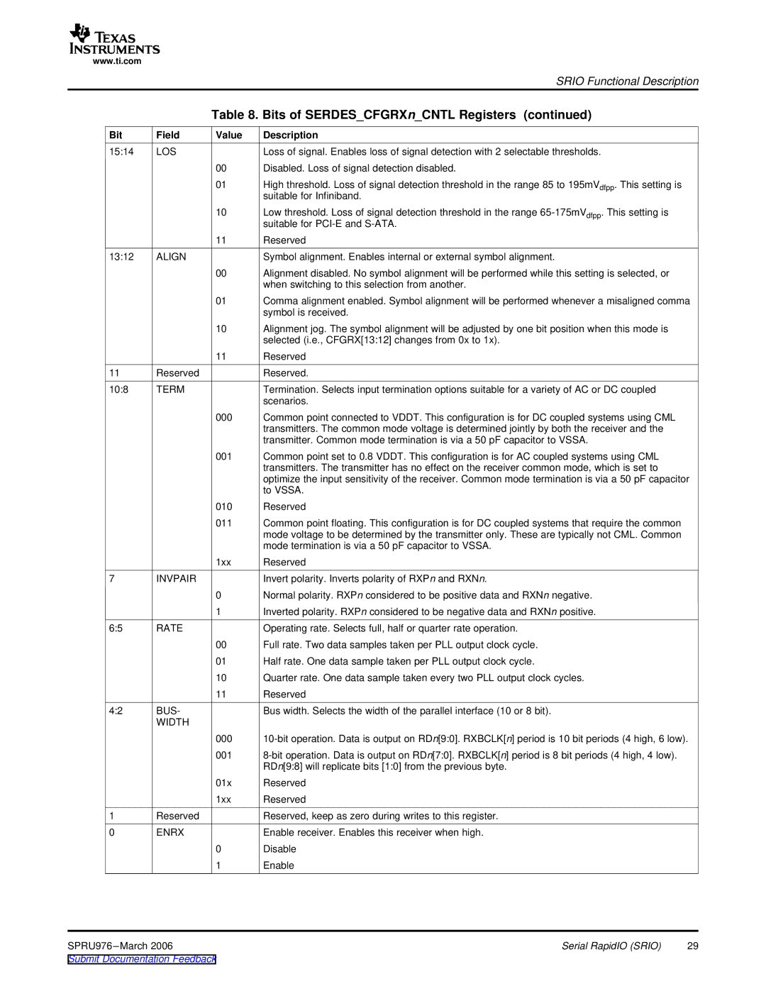
Table 8. Bits of SERDES_CFGRXn_CNTL Registers (continued)
Bit | Field | Value | Description |
15:14 | LOS |
| Loss of signal. Enables loss of signal detection with 2 selectable thresholds. |
|
| 00 | Disabled. Loss of signal detection disabled. |
01High threshold. Loss of signal detection threshold in the range 85 to 195mVdfpp. This setting is suitable for Infiniband.
| 10 | Low threshold. Loss of signal detection threshold in the range |
|
| suitable for |
| 11 | Reserved |
13:12 | ALIGN | Symbol alignment. Enables internal or external symbol alignment. |
| 00 | Alignment disabled. No symbol alignment will be performed while this setting is selected, or |
|
| when switching to this selection from another. |
01Comma alignment enabled. Symbol alignment will be performed whenever a misaligned comma symbol is received.
| 10 | Alignment jog. The symbol alignment will be adjusted by one bit position when this mode is |
|
| selected (i.e., CFGRX[13:12] changes from 0x to 1x). |
| 11 | Reserved |
11 | Reserved | Reserved. |
10:8 | TERM | Termination. Selects input termination options suitable for a variety of AC or DC coupled |
|
| scenarios. |
000Common point connected to VDDT. This configuration is for DC coupled systems using CML transmitters. The common mode voltage is determined jointly by both the receiver and the transmitter. Common mode termination is via a 50 pF capacitor to VSSA.
001Common point set to 0.8 VDDT. This configuration is for AC coupled systems using CML transmitters. The transmitter has no effect on the receiver common mode, which is set to optimize the input sensitivity of the receiver. Common mode termination is via a 50 pF capacitor to VSSA.
010 | Reserved |
011Common point floating. This configuration is for DC coupled systems that require the common mode voltage to be determined by the transmitter only. These are typically not CML. Common mode termination is via a 50 pF capacitor to VSSA.
| 1xx | Reserved |
7 | INVPAIR | Invert polarity. Inverts polarity of RXPn and RXNn. |
| 0 | Normal polarity. RXPn considered to be positive data and RXNn negative. |
| 1 | Inverted polarity. RXPn considered to be negative data and RXNn positive. |
6:5 | RATE | Operating rate. Selects full, half or quarter rate operation. |
| 00 | Full rate. Two data samples taken per PLL output clock cycle. |
| 01 | Half rate. One data sample taken per PLL output clock cycle. |
| 10 | Quarter rate. One data sample taken every two PLL output clock cycles. |
| 11 | Reserved |
4:2 | BUS- | Bus width. Selects the width of the parallel interface (10 or 8 bit). |
| WIDTH |
|
| 000 |
001
| 01x | Reserved |
| 1xx | Reserved |
1 | Reserved | Reserved, keep as zero during writes to this register. |
0 | ENRX | Enable receiver. Enables this receiver when high. |
| 0 | Disable |
| 1 | Enable |
SPRU976 | Serial RapidIO (SRIO) | 29 |
Submit Documentation Feedback |
|
|