www.ti.com
SRIO Functional Description
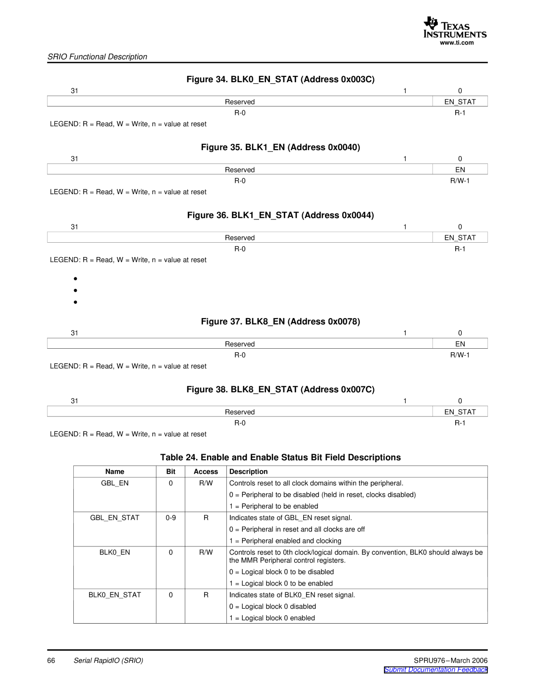
Figure 34. BLK0_EN_STAT (Address 0x003C)
31 | 1 | 0 |
Reserved |
| EN_STAT |
| ||
LEGEND: R = Read, W = Write, n = value at reset |
|
|
Figure 35. BLK1_EN (Address 0x0040)
31 | 1 | 0 |
Reserved |
| EN |
| ||
LEGEND: R = Read, W = Write, n = value at reset |
|
|
Figure 36. BLK1_EN_STAT (Address 0x0044)
31 | 1 | 0 |
Reserved |
| EN_STAT |
| ||
LEGEND: R = Read, W = Write, n = value at reset |
|
|
∙
∙
∙
Figure 37. BLK8_EN (Address 0x0078)
31 | 1 | 0 |
Reserved |
| EN |
| ||
LEGEND: R = Read, W = Write, n = value at reset |
|
|
Figure 38. BLK8_EN_STAT (Address 0x007C)
31 | 1 | 0 |
Reserved |
| EN_STAT |
|
LEGEND: R = Read, W = Write, n = value at reset
Table 24. Enable and Enable Status Bit Field Descriptions
Name | Bit | Access | Description | |
GBL_EN | 0 | R/W | Controls reset to all clock domains within the peripheral. | |
|
|
| 0 | = Peripheral to be disabled (held in reset, clocks disabled) |
|
|
| 1 | = Peripheral to be enabled |
GBL_EN_STAT | R | Indicates state of GBL_EN reset signal. | ||
|
|
| 0 | = Peripheral in reset and all clocks are off |
|
|
| 1 | = Peripheral enabled and clocking |
BLK0_EN | 0 | R/W | Controls reset to 0th clock/logical domain. By convention, BLK0 should always be | |
|
|
| the MMR Peripheral control registers. | |
|
|
| 0 | = Logical block 0 to be disabled |
|
|
| 1 | = Logical block 0 to be enabled |
BLK0_EN_STAT | 0 | R | Indicates state of BLK0_EN reset signal. | |
|
|
| 0 | = Logical block 0 disabled |
|
|
| 1 | = Logical block 0 enabled |
66 | Serial RapidIO (SRIO) | SPRU976 |
|
| Submit Documentation Feedback |