www.ti.com
SRIO Functional Description
2.2SRIO Pins
The SRIO device pins are
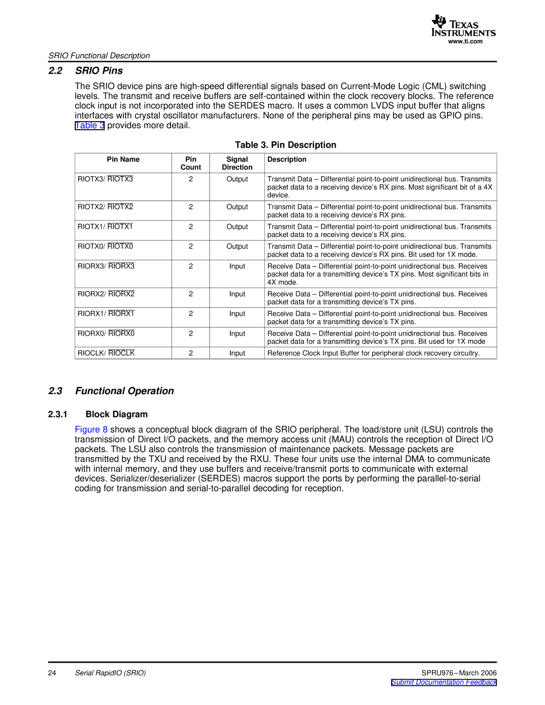
Table 3. Pin Description
Pin Name | Pin | Signal | Description |
| Count | Direction |
|
RIOTX3/ RIOTX3 | 2 | Output | Transmit Data – Differential |
|
|
| packet data to a receiving device’s RX pins. Most significant bit of a 4X |
|
|
| device. |
RIOTX2/ RIOTX2 | 2 | Output | Transmit Data – Differential |
|
|
| packet data to a receiving device’s RX pins. |
RIOTX1/ RIOTX1 | 2 | Output | Transmit Data – Differential |
|
|
| packet data to a receiving device’s RX pins. |
RIOTX0/ RIOTX0 | 2 | Output | Transmit Data – Differential |
|
|
| packet data to a receiving device’s RX pins. Bit used for 1X mode. |
RIORX3/ RIORX3 | 2 | Input | Receive Data – Differential |
|
|
| packet data for a transmitting device’s TX pins. Most significant bits in |
|
|
| 4X mode. |
RIORX2/ RIORX2 | 2 | Input | Receive Data – Differential |
|
|
| packet data for a transmitting device’s TX pins. |
RIORX1/ RIORX1 | 2 | Input | Receive Data – Differential |
|
|
| packet data for a transmitting device’s TX pins. |
RIORX0/ RIORX0 | 2 | Input | Receive Data – Differential |
|
|
| packet data for a transmitting device’s TX pins. Bit used for 1X mode |
RIOCLK/ RIOCLK | 2 | Input | Reference Clock Input Buffer for peripheral clock recovery circuitry. |
2.3Functional Operation
2.3.1Block Diagram
Figure 8 shows a conceptual block diagram of the SRIO peripheral. The load/store unit (LSU) controls the transmission of Direct I/O packets, and the memory access unit (MAU) controls the reception of Direct I/O packets. The LSU also controls the transmission of maintenance packets. Message packets are transmitted by the TXU and received by the RXU. These four units use the internal DMA to communicate with internal memory, and they use buffers and receive/transmit ports to communicate with external devices. Serializer/deserializer (SERDES) macros support the ports by performing the parallel-to-serial coding for transmission and serial-to-parallel decoding for reception.
24 | Serial RapidIO (SRIO) | SPRU976 |