www.ti.com
SRIO Functional Description
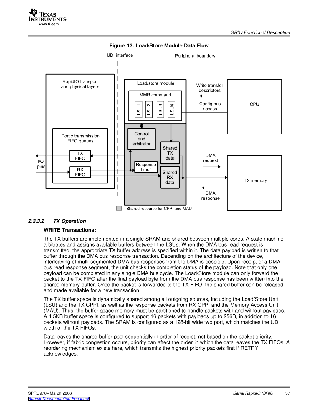
Figure 13. Load/Store Module Data Flow
UDI | Peripheral |
I/O pins
RapidIO and
Port
FIFO
TX
FIFO
RX
FIFO
Load/store
MMR |
|
| |
LSU1 | LSU2 | LSU3 | LSU4 |
Control |
|
and |
|
arbitrator | Shared |
| |
| TX |
| data |
Response |
|
timer | Shared |
| |
| RX |
| data |
Write descriptors
Config access
DMA
request
DMA
response
CPU
L2
![]()
![]() =
=
2.3.3.2TX Operation
WRITE Transactions:
The TX buffers are implemented in a single SRAM and shared between multiple cores. A state machine arbitrates and assigns available buffers between the LSUs. When the DMA bus read request is transmitted, the appropriate TX buffer address is specified within it. The data payload is written to that buffer through the DMA bus response transaction. Depending on the architecture of the device, interleaving of
The TX buffer space is dynamically shared among all outgoing sources, including the Load/Store Unit (LSU) and the TX CPPI, as well as the response packets from RX CPPI and the Memory Access Unit (MAU). Thus, the buffer space memory must be partitioned to handle packets with and without payloads. A 4.5KB buffer space is configured to support 16 packets with payloads up to 256B, in addition to 16 packets without payloads. The SRAM is configured as a
Data leaves the shared buffer pool sequentially in order of receipt, not based on the packet priority. However, if fabric congestion occurs, priority can affect the order in which the data leaves the TX FIFOs. A reordering mechanism exists here, which transmits the highest priority packets first if RETRY acknowledges.
SPRU976 | Serial RapidIO (SRIO) | 37 |