NS9215 Hardware Reference
90000847C Release date 10 April
Page
Page
Page
Contents
A p t e r 3 W o r k i n g w i t h t h e C P U
102
105
A p t e r 4 S y s t e m C o n t r o l M o d u l e 137
141
A p t e r 5 M e m o r y C o n t r o l l e r 203
Sram
Bit wide configuration 228 229
Hardware Reference NS9215
HT1
315
A p t e r 7 E x t e r n a l D M a 339
Hardware Reference NS9215
A p t e r 9 I / O H u b M o d u l e 363
Hardware Reference NS9215
A p t e r 1 1 S e r i a l C o n t r o l D u l e H D L C 415
Hardware Reference NS9215
A p t e r 1 4 R e a l T i m e C l o c k M o d u l e 459
A p t e r 1 6 T i m i n g 479
A p t e r 1 7 P a c k a g i n g 513
Hardware Reference NS9215
Pinout
Heading Description
Pin Signal Description
M o r y b u s i n t e r f a c e
N O U T 2 6
Pin Signal
H e r n e t i n t e r f a c e M a C
Sdram RAS
Sdram CAS
N e r a l p u r p o s e I / O G P I O
DCD Uart a
CTS Uart a
DSR Uart a
RXD Uart a
DCD / TXC Uart C
CTS Uart C
I2C SCL
Picdbgdataini
DCD Uart B
CTS Uart B
DSR Uart B
RXD Uart B
DSR Uart D
RXD Uart D
RI Uart D
TXC / DTR Uart D
Pin Signal Description
PIC1CLKI
PIC1CLKO
Pin Signal Description
PIC0CLKI
PIC0CLKO
Pin Signal Description
Pin Signal Description
Pin Signal Description
S t e m c l o c k
I/O OD
System clock drawing
RTC clock and battery backup drawing
S t e m m o d e
Sysmode2 Sysmode1 Sysmode0 Description
S t e m r e s e t
SPI YES
A G T e s t
Adcvss
R a n d b a t t e r y b a c k e d l o g i c
POR VSS
W e r a n d g r o u n d
GND
Power and ground
Address Description Access Reset value
N t r o l a n d S t a t u s r e g i s t e r s
System memory bus I/O control
Register address Map
Control and Status registers
I O C o n f i g u r a t i o n r e g i s t e r s
Gpio configuration options
Bits Mnemonic Description
Configuration Register #0
Configuration Register #1
Bits Access Mnemonic Reset Description
Address A0902000
Configuration Register #2
Configuration Register #3
Address A0902008
Address A090200C
Configuration Register #4
Configuration Register #5
Address A0902010
Address A0902014
Configuration Register #6
Configuration Register #7
Address A0902018
Address A090201C
Configuration Register #8
Configuration Register #9
Address A0902020
Address A0902024
Configuration Register #10
Configuration Register #11
Address A0902028
Address A090202C
Configuration Register #12
Configuration Register #13
Address A0902030
Address A0902034
Configuration Register #14
Configuration Register #15
Address A0902038
Address A090203C
Configuration Register #16
Configuration Register #17
Address A0902040
Address A0902044
Configuration Register #18
Configuration Register #19
Address A0902048
Address A090204C
Configuration Register #20
Configuration Register #21
Address A0902050
Address A0902054
Configuration Register #22
Configuration Register #23
Address A0902058
Address A090205C
Configuration Register #24
Configuration Register #25
Address A0902060
GPIOAddress A0902064
Configuration Register #26
Address A0902068
Gpio Control
I O C o n t r o l r e g i s t e r s
Address A090206C
Address A0902070
Address A0902074
Address A0902078
Gpio Status
I O S t a t u s r e g i s t e r s
Address A0902080
Address A0902084
Address A0902088
M o r y B u s C o n f i g u r a t i o n r e g i s t e r
Address A090208C
CS0
CS1
CS2
CS3
High data bus pullup control
Apudis
Memory Bus Configuration register
Working with the CPU
About the processor
Process block Diagram
S t r u c t i o n s e t s
Arm926EJ-S
ARM instruction set Thumb instruction set
Java instruction set
Accessing CP15 registers
ARM926EJ-S system addresses Address manipulation example
Terms and abbreviations
Mnemonics for these instructions are
Term Abbreviation Description
For reads
Be ZERO, does not cause any physical damage to the chip
Register summary
Register Reads Writes
TLB
This is the contents of the ID code register
Writing to register R0 is Unpredictable
R0 ID code
Any value other than 1 or 2. Note this example
Cache type register and field description
Dsize and Isize fields
Field contains these bits
Field Description
O n t r o l r e g i s t e r
Size field Cache size
Assoc field Associativity
Len field Cache line length
Bit functionality
Control register
Bits Name Function
ICache
DCache behavior
Cache
Behavior
CRm and opcode2 fields should be Zero when writing to R2
Access permissions and instructions
R a n s l a t i o n T a b l e B a s e r e g i s t e r
O m a i n a c c e s s C o n t r o l r e g i s t e r
Fault S t a t u s r e g i s t e r s
Access instructions
E g i s t e r
Register bits
Status and domain fields
Fault a d d r e s s r e g i s t e r
Priority Source Size Status Domain
A c h e O p e r a t i o n s r e g i s t e r
Function Description
Function/operation Data format Instruction
Cache operation functions
MVA
Set/Way example Test and clean DCache instructions
Modified virtual address format MVA Set/Way format
Test, clean, and invalidate DCache instruction
L B O p e r a t i o n s r e g i s t e r
Unpredictable
Operation Data Instruction
A c h e L o c k d o w n r e g i s t e r
Modified virtual address format MVA
Cache ways
That allows you to control each cache way independently
Access
Instruction or data lockdown register
Instructions
Modifying the Cache Lockdown register Register format
For each of the cache lines to be locked down in cache way
Cache unlock procedure
0 T L B L o c k d o w n r e g i s t e r
Bit
Which region the TLB entry is placed
1 a n d R 1 2 r e g i s t e r s
3 P r o c e s s I D r e g i s t e r
Programming instructions Sample code sequence
Use these instructions to program the TLB Lockdown register
Fcse PID register Access instructions
Performing a fast context switch
Register format This is the format of the Fcse PID register
Function Data ARM instruction
Context ID register Access instructions
Accessing reading or writing this register is reserved
4 r e g i s t e r
5 T e s t a n d d e b u g r e g i s t e r
MMU Features
M o r y M a n a g e m e n t U n i t M M U
State space servo control
Protection scheme
Access permissions and domains Translated entries
MMU program accessible registers Address translation
Register Bits Description
Translation table base
TTB register Format
Table walk process
First-level fetch
First-level descriptor
First-level fetch concatenation and address
Table descriptors
Bits Section Coarse Fine Description
Section descriptor Format
Value Meaning Description
Section descriptor Bit description
Fine page table
Descriptor
Bits Description
113
Second-level descriptor Second-level descriptor format
Second-level descriptor pages
Second-level descriptor least significant bits
Second-level descriptor bit assignments
Bits Large Small Tiny Description
Translation sequence for large page references
Translating sequence for small page references
Translation Sequence for tiny
References
Level descriptor
More information
U Fault s a n d C P U a b o r t s
Priority encoding table Fault Address register FAR
Domain Fault Address register
FAR values for Multi-word
Transfers
Compatibility issues
Specifying access permissions
Interpreting access permission bits
M a i n a c c e s s c o n t r o l
Fault c h e c k i n g s e q u e n c e
Privileged permissions User permissions
No access 00 Reserved Check domain status
Fault checking sequence
A b l i n g a n d d i s a b l i n g t h e M M U
T e r n a l a b o r t s
Enabling
B s t r u c t u r e
Disabling
Cache features
C h e s a n d w r i t e b u f f e r
Write buffer Enabling the caches
Bit settings
Settings
R1 register C and M bits for DCache
DCache
C h e M V a a n d S e t / W a y f o r m a t s
Description ARM926EJ-S behavior Table C Table B Bit
Generic, virtually indexed, virtually addressed cache
ARM926EJ-S
Cache format
N c a c h a b l e i n s t r u c t i o n f e t c h e s
This figure
For example, with a 4-way cache a =
Self-modifying code
AHB behavior Instruction Memory Barrier
Sample IMB sequences
Noncachable instruction fetches
Features
S i n t e r c o n n e c t i o n
S t e m b u s a r b i t e r
Ownership
Until the transaction completes
Master will not occupy the system bus
Locked bus sequence Relinquishing the bus
Split transfers Arbiter configuration example
D r e s s d e c o d i n g
Address range Size System functions
O g r a m m a b l e t i m e r s
Software watchdog timer
Master Name Hmaster30 assignment
N e r a l p u r p o s e t i m e r s / c o u n t e r s
Gptc characteristics Control field
Source clock frequency
Bit mode options
S i c P W M f u n c t i o n
A d r a t u r e d e code r f u n c t i o n
H a n c e d P W M f u n c t i o n
Sample enhanced PWM waveform
Input signals
NC No change CW Clockwise CCW Counter clockwise Err Error
Quadrature Encoding truth
CCW
Testing signals
Timer support
Monitors how far the encoder has moved Typical application
Digital filter
T e r r u p t c o n t r o l l e r
FIQ interrupts
IRQ interrupts
Vector
IRQ characteristics Interrupt sources
IRQ FIQ
Interrupt sources are assigned as shown
Interrupt ID Interrupt source
N f i g u r a b l e s y s t e m a t t r i b u t e s
L c o n f i g u r a t i o n
Configuring the powerup settings
PLL configuration and control system block diagram
O t s t r a p i n i t i a l i z a t i o n
Pin name Configuration bits
S t e m c o n f i g u r a t i o n r e g i s t e r s
Offset 3124 2316 158
155
Isaddr
System Memory Chip Select 0 Dynamic Memory Mask
N e r a l a r b i t e r C o n t r o l r e g i s t e r
C 0 , B R C 1 , B R C 2 , a n d B R C 3 r e g i s t e r s
Address A090
Register
B Error D e t e c t S t a t u s
Channel enable bit
Channel allocation Register Register bit assignment
This is how the channels are assigned in the four registers
Address A090 001C
EDS1
Not reset CPU instruction error
Not reset CPU data error
Not reset AHB error response
Transaction type write or read
AHB Error Interrupt Clear
AHB Slave Error Response Detect Config
M e r M a s t e r C o n t r o l r e g i s t e r
EIC
Timer 9 reload step enable
Timer 9 low step enable
Timer 9 high step enable
Timer 8 reload step enable
M e r 0 4 C o n t r o l r e g i s t e r s
Addresses A090 0190 / 0194 / 0198 / 019C / 01A0
Timer enable
Capture and compare mode functions
Debug mode
Timer clock select
M e r 5 C o n t r o l r e g i s t e r
Address A090 01A4
Reload mode
TM2
M e r 6 9 C o n t r o l r e g i s t e r s
Addresses A090 01A8 / 01AC / 01B0 / 01B4
D3118 Reserved D1716
M e r 6 9 H i g h r e g i s t e r s
M e r 6 9 L o w r e g i s t e r s
M e r 6 9 H i g h a n d L o w S t e p r e g i s t e r s
M e r 6 9 R e l o a d S t e p r e g i s t e r s
High step direction
High step
Reload step direction
Reload step
M e r 0 9 R e a d a n d C a p t u r e r e g i s t e r
Interrupt Vector Address register
Individual register mapping
Register 3124 2316 1508 0700
Interrupt enable
A D D R r e g i s t e r
Invert
Interrupt type
Interrupt service routine address
T e r r u p t S t a t u s a c t i v e
Interrupt status active
ISA
T e r r u p t S t a t u s R a w
F t w a r e W a t c h d o g C o n f i g u r a t i o n
Address A090 016C
Israw
Software watchdog enable
Software watchdog timer clock select
F t w a r e W a t c h d o g T i m e r
Software watchdog interrupt clear
O c k C o n f i g u r a t i o n r e g i s t e r
Watchdog timer
Address A090 017C
Clock scale control
Max clock scale control
CPU clock select
Memory clock out
IO hub
D u l e R e s e t r e g i s t e r
Ethernet MAC
Module Reset register resets each module on the AHB bus
Reset status
RST Stat
I2C
Miscellaneous System Configuration and Status register
Boot mode
Endian mode
Misaligned bus address response mode
Internal register access mode bit
PLL frequency formula Register Register bit assignment
L C o n f i g u r a t i o n r e g i s t e r
PLL bypass
W e r M a n a g e m e n t
Address A090 018C
Intid
Interrupt ID
Deprecated Chip sleep enable
New designs should not use this bit
Hardware clock scale control
Sdram self refresh control
CPU wake interrupt clear
RTC wakeup
I2C wakeup
SPI wakeup
Address A090 022C
B B u s a c t i v i t y S t a t u s
Addresses A090 01D0 / 01D4
Chip select 0 disable
Registers
Addresses A090 01D8 / 01DC
Chip select 0 base
Addresses A090 01E0 / 01E4
Chip select 1disable
Chip select 1 base
Addresses A090 01E8 / 01EC
Chip select 2 disable
Chip select 2 base
Addresses A090 01F0 / 01F4
Chip select 3 disable
Chip select 3 base
Addresses A09001F8 / 01FC
Chip select 0 mask
Chip select 1 disable
Addresses A090 0200
Addresses A090 0208 / 020C
N I D r e g i s t e r
Genid
STS
Status
CLR
RTC standby mode status
C M o d u l e C o n t r o l r e g i s t e r
RTC Module Control register controls the RTC module
Polarity
RTC standby mode
RTC clock ready interrupt status
RTC module interrupt status
RTC clock ready interrupt clear
RTC Module Control register
Memory controller provides these features
With and without asynchronous page mode
Static memory features, such as
Amba 32-bit AHB compliancy
W p o w e r o p e r a t i o n
Power-on reset memory map
M o r y m a p
Example Boot from flash Sdram remapped after boot
Device Write protect Mode Buffer
A t i c m e m o r y c o n t r o l l e r
ROM
Sram
Write protection Extended wait transfers
Be aware
A t i c m e m o r y i n i t i a l i z a t i o n
Access sequencing and memory width Wait state generation
Memory mapped peripherals
Programmable enable
Output enable programmable delay
A t i c m e m o r y r e a d c o n t r o l
ROM, SRAM, and Flash
External memory read transfer with zero wait states
External memory read transfer with two wait states
Timing parameter Value
WAITRD2 WAITOEN0 WAITPAGEN/A WAITWRN/A
External memory read transfers with zero wait states
WAITENN/A WAITTURNN/A
Burst of zero wait states with fixed length
Burst of two wait states with fixed length
External memory page mode read transfer
Y n c h r o n o u s p a g e m o d e r e a d
External memory 32-bit burst read from 8-bit memory
WAITRD2 WAITOEN0 WAITPAGE1 WAITWRN/A WAITWENN/A WAITTURNN/A
Timing parameters Value
WAITRD0 WAITOEN0 WAITPAGE0 WAITWRN/A WAITWENN/A WAITTURNN/A
Write enable programming delay
A t i c m e m o r y w r i t e c o n t r o l
Wait states added between external read and write transfers
External memory write transfer with zero wait states
External memory write transfer with two wait states
WAITRDN/A WAITOENN/A WAITPAGEN/A WAITWR0 WAITWEN0 WAITTURN0
S t u r n a r o u n d
S t u r n a r o u n d T i m i n g a n d p a r a m e t e r s
Read followed by write with no turnaround
WAITRD0 WAITOEN0 WAITPAGEN/A WAITWR0 WAITWEN0 WAITTURN0
Write followed by a read with no turnaround
Read followed by a write with two turnaround cycles
T e l a n e c o n t r o l
WAITRD0 WAITOEN0 WAITPAGEN/A WAITWR0 WAITWEN0 WAITTURN2
D r e s s c o n n e c t i v i t y
Memory banks constructed from 16-or 32-bit memory devices
Memory banks constructed from 16-bit memory
2Mx32 ROM
N a m i c m e m o r y c o n t r o l l e r
Access sequencing and memory width
R a M I n i t i a l i z a t i o n
Left-shift value -bit wide data bus Sdram RBC
Device size Configuration Load Mode register left shift
Bit Parameter Parameter description
256M 8M x 16M x 32M x 512M 64M x
Bit wide Configuration
Signal 16M device 64M device 128M 256M 512M
Device Signal
Left-shift value -bit wide data bus Sdram BRC
BA0
BA1
G i s t e r s
Register map
Only. Bursting is not allowed
Address Register Description
TRWL, tRDL
N t r o l r e g i s t e r
Reset values
Address A070
Bits Access Mnemonic Description
Low-power mode
Memory controller enable
Address mirror
A t u s r e g i s t e r
N f i g u r a t i o n r e g i s t e r
Self-refresh acknowledge Srefack
Write buffer status
N a m i c M e m o r y C o n t r o l r e g i s t e r
END
Sync/Flash reset/power down signal dypwrn
Dynamic memory clock enable
Sdram initialization
Self-refresh request Srefreq
Refresh timer
Refresh
Read data strategy
Active to precharge command period tRAS
Precharge command period tRP
RAS
Srex
Address A070 003C
Self-refresh exit time tSREX
Last-data-out to active command time tAPR
APR
Data-in to active command tDAL or tAPW
DAL
Active to active command period tRC
Address A070 004C
RFC
Auto-refresh period and auto-refresh to active command
Period
Exit self-refresh to active time command
XSR
Load mode register to Active Command Time
RRD
Active Bank a to Active Bank B
MRD
External wait timeout
A t i c M e m o r y E x t e n d e d W a i t r e g i s t e r
Example
Address A070 0100 / 0120 / 0140
Write protect
Bdmc
Address mapping
AM1
Memory Configuration
Address mapping
For the Dynamic
119 Description
Address A070 0104 / 0124 / 0144
For a chip select connected to Select this mapping
RAS latency active to read/write delay
CAS
CAS latency
Do not modify
Buffer enable
Psmc
Bsmc
Extended wait
Chip select polarity
Byte lane state
Mode
Bmode
Burst mode
Memory width
Wait write enable Waitwen
Wait output enable Waitoen
Address A070 0208 / 0228 / 0248
Wwen
Nonpage mode read wait states or asynchronous page mode
Read first access wait state Waitrd
A t i c M e m o r y R e a d D e l a y 0 3 r e g i s t e r s
Wtrd
Asynchronous page mode read after the first wait state
Wtpg
Wtwr
Address A070 0218 / 0238 / 0258
Write wait states Waitwr
Wttn
Bus turnaround cycles Waitturn
StaticMemory Turn Round Delay 0-3 registers
Features Common acronyms
Ethernet Communication Module
H e r n e t M a C
Ethernet communications module
MAC module block diagram Features
Feature Description
A t i o n a d d r e s s l o g i c S a L
PHY interface mappings
Station address logic
Media Independent Interface
A t i s t i c s m o d u l e
MAC receiver
Ethernet front- end module EFE
H e r n e t f r o n t e n d m o d u l e
Receive packet processor
C e i v e p a c k e t p r o c e s s o r
Transmit packet processor
Receive buffer descriptor format
Transferring a frame to system memory
Receive buffer descriptor format description
A n s m i t p a c k e t p r o c e s s o r
Receive buffer descriptor field definitions
Transmit buffer Descriptor field
Transmit buffer descriptor format
Definitions
Transmitting a frame
Frame
Transmitted
Successfully
Unsuccessfully
T e r r u p t s
H e r n e t s l a v e i n t e r f a c e
Interrupt condition Description
S e t s
Bit field Register Active Default Modules reset State
Status bits
L t i c a s t a d d r e s s f i l t e r i n g
Filter entries
Multicast address Filter registers
Multicast address filtering example
O c k s y n c h r o n i z a t i o n
Multicast address
Filtering example
Writing to other registers
Register address Filter
Rxdptr
Eintr
Eintren
Txptr
H e r n e t G e n e r a l C o n t r o l R e g i s t e r #
Address A060
Enable RX packet processing
Enable receive DMA
Enable TX packet processing
Accept short 64 receive frames
Enable transmit DMA
Enable initialization of RX buffer descriptors
Etxdma
Erxinit
MAC host interface soft reset
RX Fifo RAM access
Align RX data
Insert transmit source address
H e r n e t G e n e r a l S t a t u s r e g i s t e r
Rxinit
H e r n e t T r a n s m i t S t a t u s r e g i s t e r
RX initialization complete
Frame transmitted OK
Broadcast frame transmitted
Multicast frame transmitted
TX abort late collision
H e r n e t R e c e i v e S t a t u s r e g i s t e r
Address A060 001C
Receive frame size in bytes
Receive frame OK
Receive broadcast frame
Receive multicast frame
C C o n f i g u r a t i o n R e g i s t e r #
Receive enable
Bits Access Mnemonic Reset Definition
Internal loopback
Excess deferral
Auto detect pad enable
Vlan pad enable
Pad/CRC enable
CRC enable
C k t o B a c k I n t e r P a c k e t G a p r e g i s t e r
PAD operation Table for transmit
Frames
Type
Full-duplex mode
Half-duplex mode
Address A060 040C
Back-to-back inter-packet-gap
L l i s i o n W i n d o w / R e t r y r e g i s t e r
Address A060
IPGR1
Non back-to-back inter-packet-gap part
X i m u m F r a m e r e g i s t e r
Cwin
Collision window
Retx
Maximum frame length
Reset MII management block
Rmiim
Clocks field Settings
I M a n a g e m e n t C o m m a n d r e g i s t e r
Clock select
Suppress preamble
I M a n a g e m e n t a d d r e s s r e g i s t e r
Register bit
If both Scan and Read are set, Scan takes precedence
Automatically scan for read data
I M a n a g e m e n t R e a d D a t a r e g i s t e r
I M a n a g e m e n t W r i t e D a t a r e g i s t e r
Address A060 042C
I M a n a g e m e n t I n d i c a t o r s r e g i s t e r
MII read data
Miilf
MII link failure
A t i o n a d d r e s s r e g i s t e r s
Read data not valid
Nvalid
Automatically scan for read data in progress
A t i o n a d d r e s s F i l t e r r e g i s t e r
Register bit assignments for all three registers
Station Address Register #1
Station Address Register #2
G i s t e r H a s h T a b l e s
PRO
PRM
PRA
Address Register Transmit and receive counters
A t i s t i c s r e g i s t e r s
TR1K
Receive statistics Counters address
Receive byte counter A060 069C
Receive packet counter A060 06A0
Address Register Receive counters
Receive FCS error counter A060 06A4
Receive multicast packet counter A060 06A8
Receive broadcast packet counter A060 06AC
Rbuo
Receive alignment error counter A060 06BC
Receive code error counter A060 06C4
Receive carrier sense error counter A060 06C8
Receive undersize packet counter A060 06CC
Receive jabber counter A060 06D8
Transmit statistics counters address map
Transmit byte counter A060 06E0
Address Register Transmit counters
Transmit packet counter A060 06E4
Transmit excessive collision packet counter A060
Transmit oversize frame counter A060
Transmit undersize frame counter A060
These are the General Statistics registers
Carry Register
C1MAX
C1MGV
C1RBY
C1RPK
Mask register
M1MGV
M1RBY
M1RPK
M1RFC
Address A060 073C
Mask register Register
0x00000000 RXA Buffer Descriptor Pointer
Address A060 0A04
RXB Buffer Descriptor Pointer
Address A060 0A08
Address A060 0A0C
RXC Buffer Descriptor Pointer
RXD Buffer Descriptor Pointer
H e r n e t I n t e r r u p t S t a t u s r e g i s t e r
Address A060 0A10
Rxovflstat
Rxbufc
Rxdoneb
Rxdonec
Rxdoned
Rxnobuf
H e r n e t I n t e r r u p t E n a b l e r e g i s t e r
Address A060 0A14
Address A060 0A18
Address A060 0A1C
Address A060 0A20
Address A060 0A24
Address A060 0A28
Address A060 0A2C
Address A060 0A30
Address A060 0A34
Address A060 0A38
F r e e B u f f e r r e g i s t e r
Address A060 0A3C
Rxfreed
Rxfreec
L t i c a s t a d d r e s s F i l t e r r e g i s t e r s
Address A060 0A58
Address A060 0A5C
Address A060 0A60
Address A060 0A64
L t i c a s t a d d r e s s M a s k r e g i s t e r s
Address A060 0A90
Address A060 0A94
Address A060 0A98
Address A060 0A9C
Address A060 0AB4
Address A060 0AB8
Address A060 0ABC
Address A060 0AC0
B u f f e r D e s c r i p t o r R a M
Offset+0
Offset+4
Offset+8
Offset+C
Address A060 2000 512 locations
M p l e h a s h t a b l e code
Pointer to buffer to store hash table
Pointer to hash table
337
Sample hash table code
External DMA
A t r a n s f e r s
DMA buffer descriptor diagram
A b u f f e r d e s c r i p t o r
Source address pointer Buffer length
Destination
S c r i p t o r l i s t p r o c e s s i n g
Use this equation to compute total access time
R i p h e r a l D M a r e a d a c c e s s
Determining the width of Pden Equation variables
Variable Definition
Peripheral DMA burst read access
Peripheral DMA single read access
R i p h e r a l D M a w r i t e a c c e s s
Peripheral DMA burst write access
REQ signal
REQ signal
Logic remains paused until the REQ signal is reasserted
Done signal Special circumstances
Static ram chip select configuration
A t i c R a M c h i p s e l e c t c o n f i g u r a t i o n
Register name Field Value Comment
A B u f f e r D e s c r i p t o r P o i n t e r
A C o n t r o l r e g i s t e r
Channel enable
Channel go
Source width
Destination width
Destination burst
Fly-by mode
Source address increment
State
Reset
Index
Error completion interrupt pending
Normal completion interrupt pending
Buffer not ready interrupt pending
Channel abort interrupt pending
A P e r i p h e r a l C h i p S e l e c t r e g i s t e r
SEL
Chip select
DMA Peripheral Chip Select register
AES
Processes 32 bits at a time
Is programmable for 128-, 192-, or 256-bit key lengths
Supports ECB, CBC, OFB, CTR, and CCM cipher modes
Block diagram
Key size Characteristic 128 192 256
S D M a b u f f e r d e s c r i p t o r
Data blocks
AES buffer descriptor diagram
Source address pointer
Source buffer length
Destination buffer length
AES op code
Interrupt I bit Last L bit Full F bit
C r y p t i o n
B p r o c e s s i n g
C , C F B , O F B , a n d C T R p r o c e s s i n g
CCM mode does not require an initialization vector
M m o d e
Nonce buffer
Contents
Bits
CCM mode
Hub Module
A c o n t r o l l e r
AHB slave
Interface
Servicing RX and FIFOs
Source address pointer Buffer length Control15 W
Control14
Control13 L
Control12 F
Control110
Status150
A n s m i t D M a e x a m p l e
Not applicable
Process
Pointer and Index
Visual example
System Memory
Reserved
Uart a register Address map
Uart B register Address map
Register Offset Description
Uart C register Address map
Uart D register Address map
SPI register Address map
AD register Address map
Reserved
I2C register Address map
IO Hardware Assist register
RTC register Address map
IO register Address map
Error completion interrupt pending RX
Normal completion interrupt pending RX
Buffer not ready interrupt pending RX
Channel abort interrupt pending RX
RX Fifo service request interrupt pending
Error completion interrupt pending TX
TX Fifo service request interrupt pending
RX Fifo overflow interrupt pending
D u l e D M a R X C o n t r o l
Flex I/O
Channel abort
Direct
Rxthrs
Rxbdp
RX Fifo threshold
D u l e D i r e c t M o d e R X S t a t u s F I F O
D u l e D i r e c t M o d e R X D a t a F I F O
Full flag
D u l e D M a T X C o n t r o l
Indexen
Txbdp
D u l e D i r e c t M o d e T X D a t a F I F O
TX Fifo threshold
TXD
D u l e D i r e c t M o d e T X D a t a L a s t F I F O
Txdl
384
Modem control signal support
Receive error conditions
Character gap timeout
DMA transfers to and from system memory
Example configuration
R m a l m o d e o p e r a t i o n
Uart module structure
Control register Field Value Comment
U d r a t e g e n e r a t o r
Baud rates
This table shows the baud rates achieved with CLKref set to
Divisor Baud rate
R d w a r e b a s e d f l o w c o n t r o l
R c e d c h a r a c t e r t r a n s m i s s i o n
Force character transmission procedure Collecting feedback
M w a k e u p o n c h a r a c t e r r e c o g n i t i o n
A p p e r C o n t r o l a n d S t a t u s r e g i s t e r s
Address Register
DLAB=0
DLAB=1
A p p e r C o n f i g u r a t i o n r e g i s t e r
Rtsen
RTS
Dtren
Software
Receive character-based flow control
Remote loopback
RTS control
Enable force complete
T e r r u p t E n a b l e r e g i s t e r
RS485 transceiver deassertion control
RS485 transceiver assertion control
Enable overflow error
Enable parity error
Enable frame error
Enable line break
T e r r u p t S t a t u s r e g i s t e r
Parity error
Frame error
Uart interrupt
Force complete
Ring indicator
Character match3
Character match2
Character match1
Enable receive character gap timer
Transmit idle
Receive idle
Write this field to
Enable transmit bit rate generation
C e i v e B u f f e r G a P C o n t r o l r e g i s t e r
Mask
Enable character match
Data
Flow control enable
Flowstate
Flow control state
FLOW4
FLOW2
Force transmit enable
M W a k e u p C o n t r o l r e g i s t e r
Read-only busy
Char
Enable
A n s m i t B y t e C o u n t
Address 90011034 / 90019034 / 90021034
Txcount
R T T r a n s m i t B u f f e r
R T R e c e i v e B u f f e r
Rbuff
R T B a u d R a t e D i v i s o r L S B
R T B a u d R a t e D i v i s o r M S B
Tbuff
Brdl
Enables modem status interrupt
R T I n t e r r u p t E n a b l e r e g i s t e r
Brdm
Edssi
Enables receive line status interrupt
Enables transmit holding register empty interrupt
Enables receive data available interrupt
Interrupt identification
Enable the TX and RX Fifo
R T F I F O C o n t r o l r e g i s t e r
R T L i n e C o n t r o l r e g i s t e r
Clear all bytes in the TX Fifo
Divisor latch access bit
Parity enable
Set break, if set TX data is set to
Stick parity, operates as follows
Local loopback enable bit
R T M o d e m C o n t r o l r e g i s t e r
R T L i n e S t a t u s r e g i s t e r
Automatic flow control
R T M o d e m S t a t u s r e g i s t e r
Delta DCD indicator
Trailing edge of RI indicator
Delta DSR indicator
Delta CTS indicator
Uart Modem Status register
C e i v e a n d t r a n s m i t o p e r a t i o n s
Hdlc module structure
O c k i n g
T s
Transmit operation
Transmitter underflow
T a e n c o d i n g
Last byte bit Pattern table
Encoding examples
Last byte bit pattern Valid data
Transitions
Dpll operation Adjustment ranges and output clocks
NRZ and Nrzi encoding Biphase-Level encoding
CLK
Address
Received or a buffer close event occurs, such as end
Enable Hdlc interrupt
Enable invalid CRC
Enable valid CRC
Local loopback
Enable receive abort error
Rabort
Receive abort error
Hdlc interrupt
Invalid CRC
Valid CRC
L C D a t a R e g i s t e r
Hdata
Hdata
Hmode
L C C o n t r o l R e g i s t e r
Clock source
L C C l o c k D i v i d e r L o w
Address 9002911C
L C C l o c k D i v i d e r H i g h
Divl
Clock enable
Divh
Four-wire interface RXD, TXD, CLK, CS
Programmable SPI mode 0, 1, 2, or
Master mode internal diagnostic loopback
Interface SPI module
I c o n t r o l l e r
SPI module structure
Timing modes Clocking mode diagrams
SPI mode SPI CLK Idle
I c l o c k i n g m o d e s
Capture edge Drive edge
SPI master mode SPI slave mode
I c l o c k g e n e r a t i o n
S t e m b o o t o v e r S P I o p e r a t i o n
Clock generation samples
Bootmode10 Address width
Available Strapping options
EEPROM/FLASH header
Entry Name
Time to completion
Entry Name Description
Configuration registers for the SPI module are located at
This is the primary SPI Configuration register
Enable master loopback mode
I C o n t r o l a n d S t a t u s r e g i s t e r s
SPI mode
Slave enable
O c k G e n e r a t i o n r e g i s t e r
Discard bytes
Bits Access Mnemonic Reset Divisor
Enable clock generation
Register programming steps
Use this register to define the data rate of the interface
D3102 Not used Write this field to D01
SPI master timing Parameters
I t i m i n g c h a r a c t e r i s t i c s
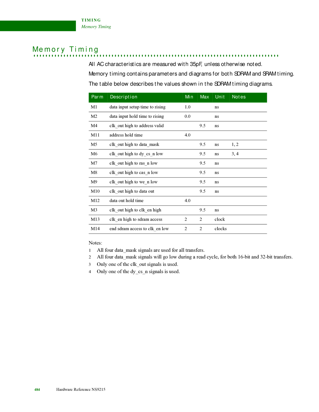
Parm Description Min Max Unit
SPI master timing diagram SPI slave timing parameters
SPI slave timing diagram
SPI timing characteristics
Interface timing, data structure, and error handling
Y s i c a l I 2 C b u s
I2C bus
Overview
E x t e r n a l a d d r e s s e s
Slave Description Addres Bit
Command Name Description
C o m m a n d i n t e r f a c e
R e g i s t e r s
M m a n d T r a n s m i t D a t a r e g i s t e r
Address 9005
RegisterDescription
2C Dlen port iicdlen
A t u s R e c e i v e D a t a r e g i s t e r
Provide new transmit data
S t e r a d d r e s s r e g i s t e r
Scmdl
Mcmdl
Irqcd
A v e a d d r e s s r e g i s t e r
Timing parameter for fast-mode Register
Address 9005 000C
Mask the interrupt to the ARM CPU irqdis
Master/slave interrupt codes
T e r r u p t codes
Code Name Master/slave Description
F t w a r e d r i v e r
I2C master software driver I2C slave high level driver
O w c h a r t s
Master module normal mode, 16- bit
Slave module normal mode, 16- bit
Real Time Clock Module
C G e n e r a l C o n t r o l r e g i s t e r
Address 9006
12/24 clock mode operation
2 4 H o u r r e g i s t e r
Calendar operation
Time date, hour, minute, second operation
HRT
M e r e g i s t e r
HRU
L e n d a r r e g i s t e r
Address 9006 000C
M e Alarm r e g i s t e r
L e n d a r Alarm r e g i s t e r
Alarm E n a b l e r e g i s t e r
E n t F l a g s r e g i s t e r
Address 9006 001C
Alarm event
Month event
Date event
Hour event
Alarm interrupt
Month interrupt
Date interrupt
Hour interrupt
T e r r u p t D i s a b l e r e g i s t e r
T e r r u p t E n a b l e S t a t u s r e g i s t e r
N e r a l S t a t u s r e g i s t e r
Address 9006 002C
General Status register
ADC module
Structure
C D M a p r o c e d u r e
ADC control block
C c o n t r o l a n d s t a t u s r e g i s t e r s
ADC configuration registers are located at offset
C C o n f i g u r a t i o n r e g i s t e r
Interrupt status
DMA enable
ADC channel select
C O u t p u t R e g i s t e r s 0
C C l o c k C o n f i g u r a t i o n r e g i s t e r
Wait
Dout
E c t r i c a l c h a r a c t e r i s t i c s
Parameter Symbola Rating Unit
Absolute maximum ratings
CPU / Memory clock Power
Parameter Symbol a Rating Unit
Recommended operating conditions
Inputs
E l e c t r i c a l c h a r a c t e r i s t i c s
Sym Parameter Conditiona Value Unit
Ouputs
Sym Parameter Value Unit
Manufacturer Part Number Description
NC7SP17
74LVC1G17GW
SN74LVC1G17DC
M o r y T i m i n g
Sdram burst read 16-bit
Sdram burst read 16 bit, CAS latency =
Sdram burst write 16 bit
Sdram burst read 32 bit
Sdram burst read 32 bit, CAS latency =
Sdram burst write 32-bit
Sdram load mode
Sdram refresh mode
Clock enable timing
Parm Description Min Max Unit
Static RAM read cycles with 0 wait states
Static RAM asynchronous page mode read, Wtpg =
Static RAM read cycle with configurable wait states
Static RAM sequential write cycles
Static RAM write cycle
Static write cycle with configurable wait states
Slow peripheral acknowledge timing
CPU
Slow peripheral acknowledge read
Slow peripheral acknowledge write
Ethernet timing
Ethernet MII timing
Standard Mode Fast Mode Parm Description Min Max Unit
I2C timing
SPI Timing
Parm Description Min Max Unit Mod Not
SPI master parameters
SPI slave parameters
Tbclk *8
SPI master mode 0 and 1 2-byte transfer
SPI master mode2 and 3 2-byte transfer
SPI slave mode 0 and 1 2-byte transfer
SPI slave mode 2 and 3 2-byte transfer
S e t a n d h a r d w a r e s t r a p p i n g t i m i n g
Parm Description Min Typ Unit
A G t i m i n g
O c k t i m i n g
Diagram below pertains to clock timing
System PLL reference clock Timing
Clock timing
Packaging
C k a g e
O c e s s o r D i m e n s i o n s
C K a G I N G
Processor Dimensions
V i s i o n B
V i s i o n C