Technical Manual
Document Number X19A-Q-002-14
This page Left Blank
Customer Support Information
This page Left Blank
Memory Interface
Power Down Modes
General Purpose IO pins
CPU Interface
CPU
Ramdac
Hardware Functional Specification
Document Number X19A-A-002-18
X19A-A-002-18 Issue Date 01/01/30
Table of Contents
Registers
Display Buffer
Display Configuration 116
Power Save Modes 128
Clocking 119
This page Left Blank
List of Tables
Vancouver Design Center
List of Figures
Vancouver Design Center
Overview Description
Introduction
Scope
CPU Interface
Features
Memory Interface
Display Support
Miscellaneous
Display Modes
Clock Source
Package and Pin
Typical System Implementation Diagrams
LCD
Management MC68000
Typical System Diagram Generic Bus, 1Mx16 FPM/EDO-DRAM
Functional Block Descriptions Host Interface
Functional Block Diagram
Block Description
Memory Controller
LCD Interface
Power Save
Look-Up Table
Package type 128 pin surface mount QFP15
Pinout Diagram for S1D13504F00A
Pin Out
Pinout Diagram for S1D13504F01A
Package type 128 pin surface mount TQFP15
Pinout Diagram for S1D13504F02A
Package type 144 pin surface mount QFP20
AB0
Pin Description
Key
TS2
BS#
CS#
Busclk
RD/WR#
RESET#
WAIT# TS2
WE# CO1
LCAS# CO1
UCAS# CO1
RAS# CO1
MA9 TS1
Clock Input
LCD Interface Pin Descriptions
CRT and External Ramdac Interface
Vrtc
CRT and Ramdac Interface Pin Descriptions
Hrtc
BLANK# CN3
Power Supply
Pin # Pin Name Type Driver Description F00A F02A F01A
Summary of Configuration Options
Asym 256Kx16
Multiple Function Pin Mapping
S1D13504 SH-3 MC68K Bus Generic MPU Pin Names
Asym 1Mx16
11 LCD, CRT, Ramdac Interface Pin Mapping
Symbol Parameter Condition Min Typ Max Units
C. Characteristics
Symbol Parameter Rating Units
Output Pin Capacitance
Low Level Output Voltage
Output Leakage Current
Bidirectional Pin Capacitance
WAIT#
CPU Interface Timing 1 SH-3 Interface Timing
RD/WR# BS#
Symbol Parameter Min Max Units
T13 T14 T15 D150read
2 MC68K Bus 1 Interface Timing e.g. MC68000
AS# UDS# LDS#
D150 hold from falling edge of DTACK# write cycle
AS# high setup to CLK
AS# high to DTACK# high impedance
D150 valid to DTACK# falling edge read cycle
AS# DS#
3 MC68K Bus 2 Interface Timing e.g. MC68030
A200 SIZ10 M/R#
T13 T14 T15
D3116 hold from falling edge of DSACK1# write cycle
D3116 valid to DSACK1# falling edge read cycle
A200
Generic MPU Interface Synchronous Timing
Bclk
RD0#,RD1# WE0#,WE1# Hi-Z
Low write cycle D150 hold from WE0#, WE1# high write cycle
Hi-Z Valid T10 D150read
Generic MPU Interface Asynchronous Timing
A200 Valid
T82
Symbol Parameter Min Typ Max Units
Clock Input Requirements
Memory Interface Timing EDO-DRAM Read Timing
RAS# CAS#
EDO Dram Read Timing
EDO-DRAM Write Timing
RAS# CAS# WE#
T14 Write Data setup time 45 t1 T15 Write Data hold time
55 t1 + CAS# precharge time 45 t1
EDO-DRAM Read-Write Timing
EDO-DRAM Read-Write Timing
EDO Dram Read-Write Timing
EDO-DRAM CAS Before RAS Refresh Timing
10 EDO-DRAM CAS Before RAS Refresh Timing
EDO-DRAM Self-Refresh Timing
11 EDO-DRAM Self-Refresh Timing
FPM-DRAM Read Timing
12 FPM-DRAM Read Timing
12 FPM Dram Read Timing
FPM-DRAM Write Timing
13 FPM-DRAM Write Timing
T14 Write Data setup time 45 t1 T15 Write Data hold time
FPM-DRAM Read-Write Timing
14 FPM-DRAM Read-Write Timing
45 t1 S1D13504
FPM-DRAM CAS# Before RAS# Refresh Timing
RAS# precharge time REG22h bits 32 = 01 or 45 t1
FPM-DRAM Self-Refresh Timing
16 FPM-DRAM CBR Self-Refresh Timing
Display Interface Power-On/Reset Timing
Fpframe active
Suspend Timing
Mclk
Vndp =
Single Monochrome 4-Bit Panel Timing
VDP =
HDP =
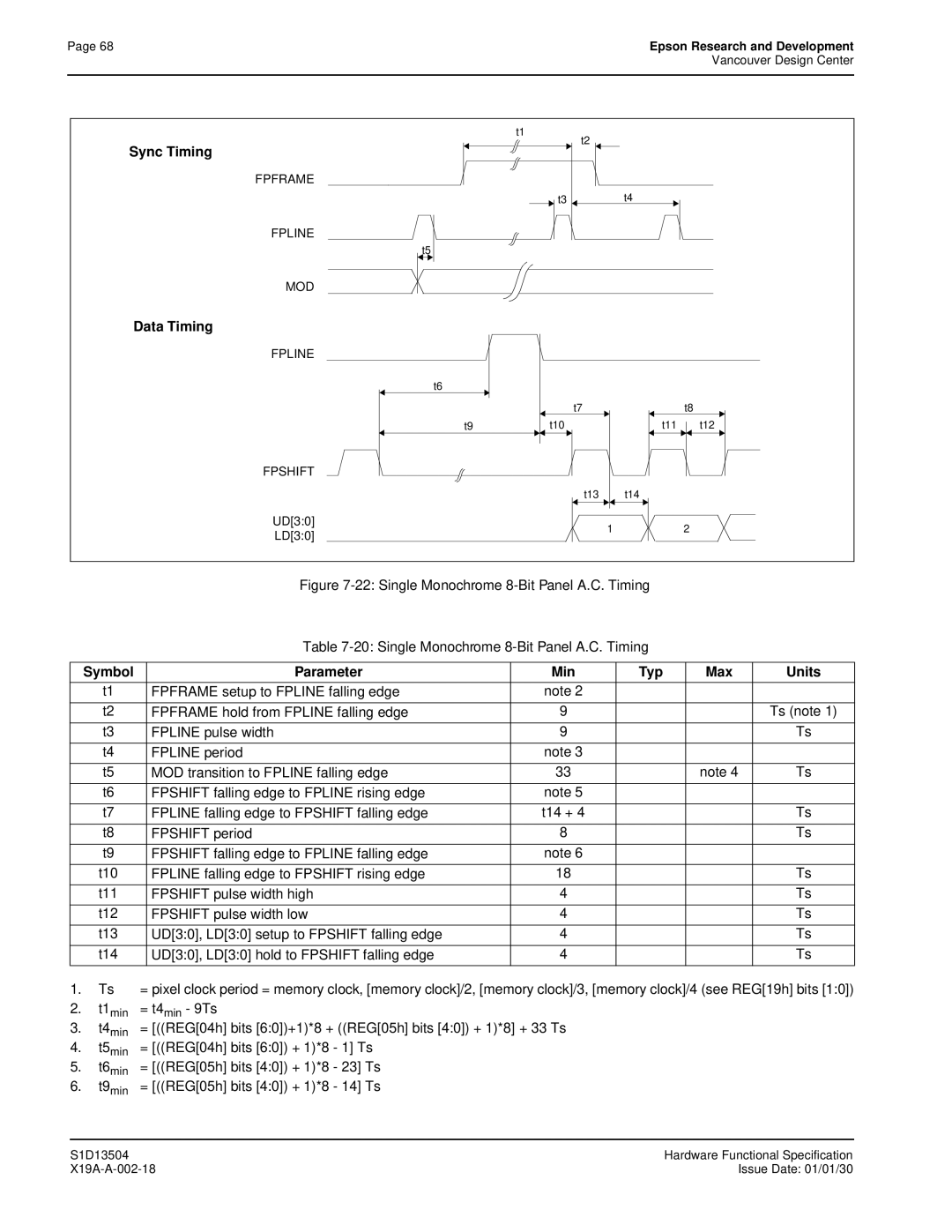
Sync Timing
Data Timing
Vndp
Single Monochrome 8-Bit Panel Timing
VDP
HDP
= REG05h bits 40 + 1*8 23 Ts
UD30, LD30 setup to Fpshift falling edge
UD30, LD30 hold to Fpshift falling edge
= REG05h bits 40 + 1*8 14 Ts
Single Color 4-Bit Panel Timing
23 Single Color 4-Bit Panel Timing
= REG05h bits 40 + 1*8 17 Ts
= REG04h bits 60+1*8 1 Ts
= REG05h bits 40 + 1*8 26 Ts
Single Color 8-Bit Panel Timing Format
25 Single Color 8-Bit Panel Timing Format
FPSHIFT2 falling edge to Fpline rising edge
UD30, LD30 setup to FPSHIFT2 rising, Fpshift falling edge
Fpline pulse width Fpline period
FPSHIFT2, Fpshift pulse width high
27 Single Color 8-Bit Panel Timing Format
T1min = t3min 9Ts
Single Color 16-Bit Panel Timing
VDP Vndp LINE1 LINE2 LINE3 LINE4 LINE479 LINE480 HDP Hndp
UD70, LD70 setup to Fpshift falling edge
UD70, LD70 hold to Fpshift falling edge
Dual Monochrome 8-Bit Panel Timing
Fpshift UD3 UD2 UD1 UD0 LD3 LD2 LD1 LD0
= REG05h bits 40 + 1*8 8 Ts
Dual Color 8-Bit Panel Timing
33 Dual Color 8-Bit Panel Timing
= REG05h bits 40 + 1*8 9 Ts
Dual Color 16-Bit Panel Timing
35 Dual Color 16-Bit Panel Timing
UD70 LD70
12 16-Bit TFT Panel Timing
= Vertical Display Period = REG09h bits 10, REG08h bits 70 +
38 TFT A.C. Timing
= REG0Ch bits 20+1 lines
= REG04h bits 60+1*8 + REG05h bits 40+1*8 Ts
= REG07h bits 30+1*8 Ts
CRT Timing
39 CRT Timing
40 CRT A.C. Timing
Dacclk period
Write
External Ramdac Read / Write Timing
Read
DACWR# pulse width low
Register Descriptions
Registers
Register Mapping
Revision Code Register
Time/256 Cycles
Memory Configuration Registers
Memory Configuration Register
MOD Rate Register
Panel/Monitor Configuration Registers
Panel Type Register
REG03h MOD Rate Bit
HRTC/FPLINE Start Position Register
Horizontal Display Width Register
Horizontal Non-Display Period Register
Hrtc Fpline
HRTC/FPLINE Pulse Width Register
Vertical Display Height Register
Vrtc Fpframe
Vertical Non-Display Period Register
VRTC/FPFRAME Start Position Register
Fpframe Vrtc
VRTC/FPFRAME Pulse Width Register
REG0Ch
Vrtc Polarity
Simultaneous Display Option Select Bits
Display Configuration Registers
Display Mode Register
Even Scan Only
Number of Bits-Per-Pixel Selection
Screen 1 Line Compare Register
Screen 1 Display Start Address Register
Memory Address Offset Register
Screen 2 Display Start Address Register 0 RW
Screen 2 Display Start Address Register
Pixel Panning Register
Clock Configuration Register
Clock Configuration Register
Number of Bits-Per-Pixel Screen 2 Pixel Panning Bits Used
Miscellaneous Disable Register
Power Save Configuration Registers
Power Save Configuration Register
Miscellaneous Registers
REG1Dh MD15 MD14 MD13 MD12 MD11 MD10
MD Configuration Readback Register
Gpio Configuration Register
MD9 MD8
Vancouver Design Center
REG1Fh GPIO11 Pin GPIO10 Pin GPIO9 Pin GPIO8 Pin IO Config
Gpio Status / Control Register
GPO
Gpio Status / Control Register
REG21h
GPIO11 Pin GPIO10 Pin GPIO9 Pin GPIO8 Pin Control IO Status
REG22h Bits
Performance Enhancement Register
REG22h EDO Read RC Timing RAS# to
Minimum Random Cycle Width t RC
REG22h Bit
RAS# to CAS# Delay tRCD
Optimal Dram Timing
RAS# Precharge Width t RP
Look-Up Table Address Register
RGB Index Bits Look-Up Table Access Pointer Sequence
Look-Up Table Registers
REG26h LUT Data Bit
Look-Up Table Data Register
Look-Up Table Bank Select Register
REG27h Red Bank Blue Bank Green Bank Select Bit
External Ramdac Control Registers
Ramdac Read Mode Address Register
Ramdac Write Mode Address Register
Ramdac Pixel Read Mask Register
Ramdac Palette Data Register
REG2Eh or REG2Fh
Display Buffer
512K byte Memory AB200
Image Buffer
Half Frame Buffer
Display Configuration
Display Mode Data Format
15/16 Bit-Per-Pixel Format Memory Organization
Image Buffer
Image Manipulation
Display
Display type
Clocking
Maximum Mclk Pclk Ratios
Maximum Pclk Allowed Bpp 16 bpp
Speed Grade Bpp Clock Hndpt s Panel
Frame Rate Calculation
= Pclk
MHz
FPM-DRAM
Look-Up Table Architecture
Bit-Per-Pixel Mode
Display Mode Bit Wide Look-Up Table
Gray Shade Display Modes
Bit-Per-Pixel Mode
Bit-Per-Pixel Color Mode
Color Display Modes
Bank Selected Bank Entry Bit Red data output Logic
Red Look-Up Table 0000 0001 0010 0011 0100 0101 Entry 0110
Color Data Format Red Look-Up Table
Software Suspend
Power Save Modes
Hardware Suspend
Power Save Mode PSM
Power Save Mode Function Summary
Pin States in Power Save Modes
Pin State Pins Normal Software Hardware Active Suspend
QFP15 128 pin Unit mm
Mechanical Data
14.1 QFP15-128 S1D13504F00A
±0.2
TQFP15-128 S1D13504F01A
TQFP15 128 pin Unit mm
125
QFP20-144 S1D13504F02A
QFP20 144 pin Unit mm
Programming Notes and Examples
Document Number X19A-G-002-07
This page Left Blank
Advanced Techniques
LCD Power Sequencing and Power Save Modes
Introduction Programming the S1D13504 Registers
Sample Code
CRT Considerations
Identifying the S1D13504 Hardware Abstraction Layer HAL
Appendix a Supported Panel Values
Initializing the S1D13504 Registers
This page Left Blank
Introduction
3 REG02 bit 1 Dual/Single Panel Type
Programming the S1D13504 Registers
2 REG22 bits 7-2 Performance Enhancement Register
Register Initialization Initialization Sequence
4 REG1B bit 0 Half Frame Buffer Disable
5 REG23 Display Fifo
Operation Description
Initialization Example
Initializing the S1D13504 Registers
Re-Programming Registers
Disabling the Half Frame Buffer Sequence
Pixel Bit
Display Buffer Location
Bit
Memory Organization for Eight Bit-per-pixel 256 Colors
Bit Red Bit Green Bit Blue Bit
Bit Reserved Red Bit Green Bit Blue Bit
Memory Organization for 15 Bit-per-pixel 32768 Colors
Memory Organization for 16 Bit-per-pixel 65536 Colors
REG26h Look-Up Table Data Register Read/Write
Look-Up Table LUT
REG24h Look-Up Table Address Register Read/Write
REG27h Look-Up Table Bank Register Read/Write
Bank Select Bits
Bank
Look-Up Table Configurations
Look-Up Table Organization
Color Modes
Recommended LUT Values for 1 bpp Color Mode
Recommended LUT Values for 2 bpp Color Mode
Address Red Green Blue
11 Recommended LUT Values For 8 bpp Color Mode
13 Recommended LUT Values for 1 bpp Gray Shades
12 Examples of 256 Pixel Colors Using Linear LUT
Gray Shade Modes
Pixel Value Color
LUT Address Green LUT Data
14 Recommended LUT Values for 2 bpp Gray Shades
15 Recommended LUT Values for 8 bpp Gray Shade
Bpp Gray Shade
Advanced Technique s
Virtual Display
REG16h Memory Address Offset Register
Registers
Examples
REG17h Memory Address Offset Register
Panning and Scrolling
Number of Pixels Panned Using Start Address
Active Pixel Pan Bits
Example 4 Panning Right and Left
Line Compare Bit
Split Screen
REG0E Screen 1 Line Compare Register
REG0F Screen 1 Line Compare Register
REG15h Screen 2 Display Start Address Register
REG13h Screen 2 Display Start Address Register
REG14h Screen 2 Display Start Address Register
Introduction to Power Save Modes
LCD Power Sequencing and Power Save Modes
Introduction to LCD Power Sequencing
Display Mode Register
Shortening the 128 Frame Delay using Hardware SUSPEND#
Suspend Enable Sequence
Shortening the 128 Frame delay using Software Suspend
Suspend Sequencing
LCD Enable / Disable using Power Save Modes
Suspend Disable Sequence
LCD Enable/Disable Sequencing Reg0D bit
LCD Enable / Disable using Manual Control
CRT Only
CRT Considerations
Introduction
Ramdac Register Mapping for Little/Big-Endian
Simultaneous Display
Related Register Data for CRT Only
Address
Address
Related register data for Simultaneous Display
Register 640X480@75Hz 640X480@60Hz
Identifying the S1D13504
Initialization Int seDeRegisterDeviceint device
Hardware Abstraction Layer HAL
API for 13504HAL
Int seGetIdint device, Byte *pId
Int seInitHalvoid
Int seValidStdDeviceint device
Int seSetInitint device
Int seValidRegisteredDeviceint device
Int seGetLastUsableByteint device, Dword *pLastByte
Int seGetBitsPerPixelint device, Byte *pBitsPerPixel
Int seGetBytesPerScanlineint device, int *pBytes
Int seGetLinearDispAddrint device, Dword *pDispLogicalAddr
Int seReadDisplayWordint device, Dword offset, Word *pWord
Int seGetScreenSizeint device, int *width, int *height
Int seReadDisplayByteint device, Dword offset, Byte *pByte
Int seSetBitsPerPixelint device, Byte BitsPerPixel
Int seSplitInitint device, Dword Scrn1Addr, Dword Scrn2Addr
Int seVirtInitint device, int xVirt, long *yVirt
Int seVirtMoveint device, Byte WhichScreen, int x, int y
Vancouver Design Center
Int seGetLutint device, Byte *pLut
Color Manipulation Int seGetDacint device, Byte *pDac
Int seGetDacEntryint device, Byte index, Byte *pEntry
Int seSetDacEntryint device, Byte index, Byte *pEntry
Int seGetLutEntryint device, Byte index, Byte *pEntry
Int seSetDacint device, Byte *pDac
Int seSetLutint device, Byte *pLut
Int seSetLutEntryint device, Byte index, Byte *pEntry
Int seDrawTextint device, char *fmt
Int sePutcint device, int ch
Int seGetcharvoid
Int sePutcharint ch
Int seSetRegint device, int index, Byte val
Miscellaneous Int seDelayint device, Dword Seconds
Int seSetPixelint device, int x, int y, Dword color
Word seRotateByteLeftBYTE val, Byte bits
Word seRotateByteRightBYTE val, Byte bits
Sample code using 13504HAL API
Sample Code
Sample code without using 13504HAL API
Vancouver Design Center
Pclk
To arrive at the frame rate closest to the desired
Words
Fifo
Passive Single Panel
Appendix a Supported Panel Values
Supported Panel Values
Passive Dual Panel
TFT Panel
TFT 16-Bit Register Single
01/02/02
Number of Bits/Pixel
13504CFG.EXE Configuration Program
Document Number X19A-B-001-04
Vancouver Design Center
X19A-B-001-04
Script Mode Interactive Mode
13504CFG.EXE Program Requirements
This page Left Blank
13504CFG View Menu
This page Left Blank
13504CFG.EXE
Usage
Installation
Program Requirements
Script Mode
Interactive Mode
13504CFG Menu Bar
Making 13504CFG Menu Selections
Files Menu
View Menu
13504CFG Current Configuration
Device Menu
Panel
Edit Panel Setup
CRT
Edit CRT Setup
Advanced Memory
Edit Advanced Memory Setup
Power Management
Edit Power Setup
Lookup Table LUT
Edit LUT Setup
Setup
Help Menu
Comments
Sample Program Messages
This page Left Blank
13504SHOW Demonstration Program
Document Number X19A-B-002-05
This page Left Blank
13504SHOW
S1D13504 Supported Evaluation Platforms
Error Too many devices registered
Program Messages
13504SPLT Display Utility
Document Number X19A-B-003-05
This page Left Blank
13504SPLT
13504SPLT Example
Comments
This page Left Blank
13504VIRT Display Utility
Document Number X19A-B-004-05
S1D13504 13504VIRT Display Utility X19A-B-004-05
13504VIRT
13504VIRT Example
Comments
This page Left Blank
13504PLAY Diagnostic Utility
Document Number X19A-B-005-05
This page Left Blank
13504PLAY
Reads/writes the registers
13504PLAY Example
Scripting
Comments
13504BMP Demonstration Program
Document Number X19A-B-006-04
This page Left Blank
13504BMP
Program Messages
13504PWR Software Suspend Power Sequencing Utility
Document Number X19A-B-007-04
X19A-B-007-04 Issue Date 01/02/01
13504PWR
Selects software suspend
Error Unknown command line argument
This page Left Blank
13504DCFG Configuration Program
Document Number X19A-B-008-02
This page Left Blank
Table of Contents
This page Left Blank
List of Figures
Clocks Tab Panel Tab
This page Left Blank
Usage
Installation
13504DCFG
13504DCFG Configuration Tabs
General Tab
General Tab
Memory Tab
Memory Tab
Clocks Tab
Clocks Tab
LCD Mclkpclk
Clocks Tab
Clki
CRT Mclkpclk
Panel Tab
Panel Tab
HRTC/FPLINE
Panel Tab
STN/TFT
VRTC/FPFRAME
CRT Tab
CRT Tab
Select the default display device. Three display modes LCD
Defaults Tab
Defaults Tab
Initializes the registers based on the default mode
Registers Tab
Registers Tab
Miscellaneous Flags Tab
Miscellaneous Flags Tab
Saving to a File
Resolution Frame Rate Hz Pclk MHz Supported Dram Types
Comments
Windows CE Display Drivers
Document Number X19A-E-001-04
X19A-E-001-04
Example Driver Builds
DIP Switch
Program Requirements
Windows Version
With this line
Build For Cepc
If CEPCDDIVGA2BPP
Epson Research and Development
Installation for Cepc Environment
Example Installation
Installation for Hitachi D9000 and Etma ODO
Comments
This page Left Blank
Wind River WindML v2.0 Display Drivers
Document Number X19A-E-002-03
X19A-E-002-03 Issue Date 01/04/06
Wind River WindML v2.0 Display Drivers
Building a WindML v2.0 Display Driver
Make CPU=PENTIUM ugl
Epson Research and Development
This page Left Blank
Wind River UGL v1.2 Display Drivers
Document Number X19A-E-003-02
X19A-E-003-02
Wind River UGL v1.2 Display Drivers
Building a UGL v1.2 Display Driver
Epson Research and Development
This page Left Blank
Document Number X19A-G-004-06
S1D13504 X19A-G-004-06 Issue Date 01/02/02
Installation and Configuration
Parts List Schematic Diagrams
This page Left Blank
S1D13504B00C Schematic Diagram 1 of 6
This page Left Blank
Features
Jumper Settings
Installation and Configuration
Configuration DIP Switch Settings
Host Bus Selection
LCD Signal Connector J6
LCD / Ramdac Interface Pin Mapping
Connector Comments Pin No
CPU / BUS Interface Connector Pinouts
CPU/BUS Connector H1 Pinout
CPU/BUS Connector H2 Pinout
Host Bus Interface Pin Mapping
DB150 D150 D3116 WE1#
Technical Description
ISA Bus Support
Decode Logic
Non-ISA Bus Support
Dram Support
Clock Input Support
Color TFT LCD Panel Support
Monochrome LCD Panel Support
Color Passive LCD Panel Support
External Cmos Ramdac Support
IO VDD Power Supply
Power Save Modes
Core VDD Power Supply
Adjustable LCD Panel Negative Power Supply
Schematic Notes
15 CPU/Bus Interface Header Strips
Parts List
Item # Qty/board Designation Part Value Description
TIBPAL22V10-15BCNT
Texas Instrument PAL 24 pin DIP package/socketed
Schematic
Diagrams
S1D13504B00C Schematic Diagram 2
Rev.1.0
S1D13504B00C Schematic Diagram 4
Diagram 5
S1D13504B00C Schematic Diagram 6
This page Left Blank
S5U13504-D9000
Document Number X19A-G-003-05
S5U13504-D9000 X19A-G-003-05 Issue Date 01/02/02
Introduction Features
D9000 Specifics
This page Left Blank
S5U13504-D9000 Perspective View
This page Left Blank
Reference
S1D13504 Color Graphics LCD Controller
Display Buffer
LCD Display Support
LCD Connector Pinout
LCD Interface Pin Mapping
Adjustable LCD Bias Power Supply
CRT Support
Interface Signals
Interface Signals
Connector Pinout for Channel A6 and A7
D9000 Specifics
DC12V
Connector Pinout for Channel A7
GND
Channel A7 Pin # Fpga Signal S1D13504 Signal SmZ
BS# GND
Connectors Pinout for Channel A6
Channel A6 Pin # Fpga Signal S1D13504 Signal SmXY
Channel A6 Pin # Fpga Signal S1D13504 Signal SmZ
Memory Address CS#, M/R# Decode
Board Dimensions
Bus Interface Timing
Makefpga file
Parts List
Item # Qty Reference Part Description
Schematic
S5U13504-D9000 Schematic Diagram 2
S5U13504-D9000 Schematic Diagram 3
D9000
PCB Layout Component Placement
Component Placement
Perspective View
S5U13504-D9000 Perspective View
Power Consumption
Document Number X19A-G-006-04
S1D13504 Power Consumption X19A-G-006-04
S1D13504 Power Consumption
Conditions
S1D13504 Total Power Consumption
Summary
Interfacing to the Philips Mips PR31500/PR31700 Processor
Document Number X19A-G-005-08
This page Left Blank
Direct Connection to the Philips PR31500/PR31700
This page Left Blank
S1D13504 to PR31500/PR31700 Connection using One IT8368E
List of Tables
This page Left Blank
Introduction
Interfacing to the PR31500/PR31700
Generic MPU Host Bus Interface Pin Mapping
WAIT# RESET#
S1D13504 Host Bus Interface
S1D13504 Generic MPU Pin Names
Generic MPU Host Bus Interface Signals
Direct Connection to the Philips PR31500/PR31700
Hardware Description
Memory Mapping and Aliasing
MD3 MD4
S1D13504 Configuration
MD1 MD2
System Design Using the IT8368E PC Card Buffer
Hardware Description-Using One IT8368E
Chip Select
Logic
Vancouver Design Center
Hardware Description-Using Two IT8368E’s
PR31500/PR31700 S1D13504
IT8368E Configuration
TX3912 Address Size Function CARDnIOEN=0 CARDnIOEN=1
IT8368E Uses PC Card Slot # Philips Address Size Function
S1D13504 Configuration using the IT8368E
Software
Document Sources
References
Documents
Philips Mips PR31500/PR31700 Processor
Technical Support
Epson LCD/CRT Controllers S1D13504
ITE IT8368E
This page Left Blank
Interfacing to the NEC VR4102 Microprocessor
Document Number X19A-G-007-07
X19A-G-007-07 Issue Date 01/02/02
Introduction Interfacing to the NEC VR4102
This page Left Blank
NEC VR4102 Read/Write Cycles
This page Left Blank
Introduction
Overview
Interfacing to the NEC VR4102
NEC VR4102 System Bus
LCD Memory Access Cycles
Lcdrdy
S1D13504 Host Bus Interface
Generic MPU Host Bus Interface Signals
Decode Logic
VR4102 to S1D13504 Interface
Read/Write
S1D13504 Hardware Configuration
Generic bus interface e.g. MPC821, ISA bus interface
WR#
NEC VR4102 Configuration
NEC Signals Cycle S1D13504 Signals
Write
Software
References
NEC Electronics Inc. VR4102
Japan North America Taiwan, R.O.C
This page Left Blank
Interfacing to the Motorola MCF5307 Coldfire Microprocessor
X19A-G-011-07 Issue Date 01/02/02
S1D13504 Bus Interface
This page Left Blank
List of Tables
This page Left Blank
Introduction
Normal Non-Burst Bus Transactions
Interfacing to the MCF5307
MCF5307 System Bus
MCF5307 Memory Read Cycle
Chip-Select Module
Burst Cycles
S1D13504 Bus Interface
Generic MPU Host Bus Interface Signals
MCF5307 To S1D13504 Interface
Hardware Connections
S1D13504 Configuration Settings
MCF5307 Chip Select Configuration
Memory/Register Mapping
Software
Motorola Inc. Motorola Literature Distribution Center, 800
Motorola MCF5307 Processor
S1D13504 Color Graphics LCD / CRT Controller
X19A-G-013-02 Issue Date 01/02/02
Introduction Interfacing to the MC68328
This page Left Blank
Generic MPU Host Bus Interface Pin Mapping
This page Left Blank
Introduction
Interfacing to the MC68328
68328 System Bus
S1D13504 Host Bus Interface
Generic MPU Host Bus Interface Signals
Busclk RESET#
MC68328 To S1D13504 Interface
CSB3 Dtack UWE LWE CLK0
MD6
MD7
MC68328 Chip Select Configuration
Option Memory Selection
Software
References
Motorola MC68328 Processor
This page Left Blank
Interfacing to the Motorola MPC821 Microprocessor
X19A-G-010-05 Issue Date 01/02/02
Introduction Interfacing to the MPC821
This page Left Blank
List of Tables
This page Left Blank
Introduction
MPC821 Bus Overview
Interfacing to the MPC821
MPC8xx System Bus
Power PC Memory Read Cycle
Power PC Memory Write Cycle
Memory Controller Module
General-Purpose Chip Select Module Gpcm
User-Programmable Machine UPM
S1D13504 Host Bus Interface
Generic MPU Host Bus Interface Signals
MPC821 to S1D13504 Interface
Typical Implementation of MPC821 to S1D13504 Interface
AB7
AB9
AB8
AB6
CS4
Sreset
Sysclk
WE0
S1D13504 Hardware Configuration
MPC821 Chip Select Configuration
Register/Memory Mapping
Test Software
Source Code
Epson Research and Development
Software
References
Motorola MPC821 Processor
Interfacing to the PC Card Bus
Document Number X19A-G-009-05
This page Left Blank
Introduction Interfacing to the PC Card Bus
This page Left Blank
PC Card Read Cycle
This page Left Blank
Introduction
PC Card System Bus
Memory Access Cycles
Interfacing to the PC Card Bus
PC Card Overview
PC Card Read Cycle
S1D13504 Host Bus Interface
Generic MPU Host Bus Interface Signals
PC Card to S1D13504 Interface
Typical Implementation of PC Card to S1D13504 Interface
SH-3
Generic MPU
PAL Equations
Equations
Software
PCMCIA/JEIDA, PC Card Standard -- March
PC Card Standard
Pcmcia
This page Left Blank
Interfacing to the Toshiba Mips TX3912 Processor
Document Number X19A-G-012-04
This page Left Blank
Direct Connection to the Toshiba TX3912
This page Left Blank
S1D13504 to TX3912 Connection using One IT8368E
This page Left Blank
Introduction
Interfacing to the TX3912
S1D13504 Host Bus Interface
Generic MPU Host Bus Interface Signals
Direct Connection to the Toshiba TX3912
Memory Mapping and Aliasing
S1D13504 Hardware Configuration
System Design Using the IT8368E PC Card Buffer
S1D13504 to TX3912 Connection using One IT8368E
Hardware Description-Using Two IT8368E’s
S1D13504 to TX3912 Connection using Two IT8368E
IT8368E Configuration
64Mb Card 1 Memory
64Mb
64Mb Card 2 Attribute
64Mb Card 2 Memory
S1D13504 Configuration
Software
References
Toshiba Mips TX3912 Processor ITE IT8368E
This page Left Blank