www.ti.com
BT.656 Video Display Mode
4.2.2 Blanking Codes
The time between the EAV and SAV code on each line represents the horizontal blanking interval. During this time, the video port outputs digital video blanking values. These values are 10.0h for luma (Y) samples and 80.0h for chroma (Cb/Cr) samples. These values are also output during the active line period of vertical blanking (between SAV and EAV when V = 1). In addition, if the DVEN bit in VDCTL is cleared to 0, the blanking values are output during the portion of active video lines that are not a part of the displayed image.
4.2.3 BT.656 Image Display
For BT.656 display mode, the FIFO buffer is divided into three sections. One FIFO is
If video display is enabled, the video display module uses the YEVT, CbEVT, and CrEVT events to notify the EDMA controller that data needs to be placed into the display FIFOs. The number of pixels required to generate the events is set by the threshold field bits in VDTHRLD register. The video display module generates the event signals when the display buffer holds less than the threshold number of pixels and the display event counter has not expired. On every YEVT, the EDMA should move data from DSP memory to the Y buffer, using the Y FIFO destination register (YDST) content as the destination address. On every CbEVT, the EDMA should move data from DSP memory to the Cb buffer, using the Cb FIFO destination register (CBDST) content as the destination address. On every CrEVT, the EDMA should move data from DSP memory to the Cr buffer, using the Cr FIFO destination register (CRDST) content as the destination address. The EDMA transfer size for the Y buffer is twice the size of the EDMA for the Cb or Cr buffers.
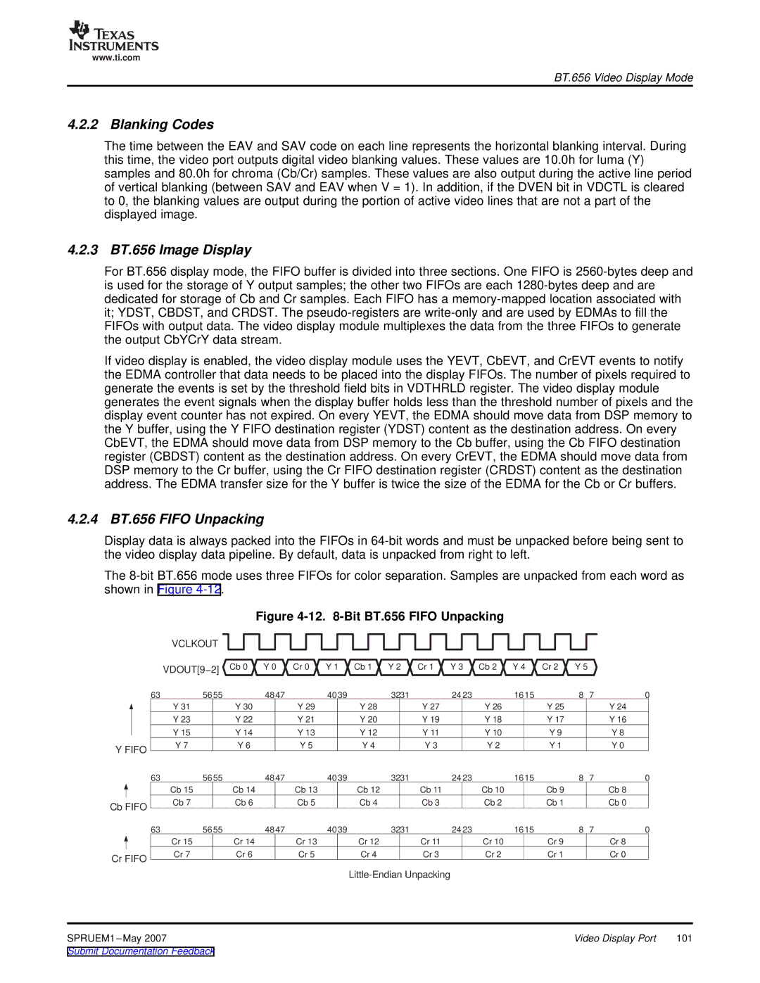
4.2.4 BT.656 FIFO Unpacking
Display data is always packed into the FIFOs in
The
Figure 4-12. 8-Bit BT.656 FIFO Unpacking
VCLKOUT
|
|
|
| VDOUT[9−2] | Cb 0 Y 0 | Cr 0 Y 1 |
| Cb 1 Y 2 | Cr 1 | Y 3 Cb 2 | Y 4 Cr 2 | Y 5 |
|
| ||||||||||||||||||||||
|
|
|
|
|
|
|
|
|
|
|
|
|
|
|
|
|
|
|
|
|
|
|
|
|
|
|
|
|
|
|
|
|
|
| ||
63 | 5655 |
|
| 4847 | 4039 | 3231 |
|
| 24 23 |
|
| 16 15 |
|
| 8 | 7 | 0 | |||||||||||||||||||
|
|
|
| Y 31 |
| Y 30 |
| Y 29 |
|
| Y 28 |
| Y 27 |
|
|
| Y 26 |
|
|
| Y 25 |
|
| Y 24 | ||||||||||||
|
|
|
|
|
| |||||||||||||||||||||||||||||||
|
|
|
| Y 23 |
| Y 22 |
| Y 21 |
|
|
| Y 20 |
|
| Y 19 |
|
|
| Y 18 |
|
|
| Y 17 |
|
| Y 16 | ||||||||||
|
|
|
| Y 15 |
| Y 14 |
| Y 13 |
|
| Y 12 |
| Y 11 |
|
|
| Y 10 |
|
|
| Y 9 |
|
| Y 8 | ||||||||||||
|
|
|
|
|
| |||||||||||||||||||||||||||||||
Y FIFO |
| Y 7 |
| Y 6 |
|
| Y 5 |
|
|
| Y 4 |
|
| Y 3 |
|
|
| Y 2 |
|
|
| Y 1 |
|
| Y 0 | |||||||||||
|
|
|
|
|
|
|
|
|
|
|
|
|
|
|
|
|
|
|
|
|
|
|
|
|
|
|
|
|
|
|
|
|
| |||
63 | 5655 | 4847 | 4039 | 3231 |
|
| 24 23 |
|
| 16 15 |
|
| 8 | 7 | 0 | |||||||||||||||||||||
|
|
|
| Cb 15 |
| Cb 14 |
| Cb 13 |
|
| Cb 12 |
| Cb 11 |
|
|
| Cb 10 |
|
|
| Cb 9 |
|
| Cb 8 | ||||||||||||
Cb FIFO |
| Cb 7 |
| Cb 6 |
| Cb 5 |
|
| Cb 4 |
| Cb 3 |
|
|
| Cb 2 |
|
|
| Cb 1 |
|
| Cb 0 | ||||||||||||||
|
|
|
|
|
|
|
|
|
|
|
|
|
|
|
|
|
|
|
|
|
|
|
|
|
|
|
|
|
|
|
|
|
| |||
63 | 5655 | 4847 | 4039 | 3231 |
|
| 24 23 |
|
| 16 15 |
|
| 8 | 7 | 0 | |||||||||||||||||||||
|
|
|
| Cr 15 |
| Cr 14 |
| Cr 13 |
|
| Cr 12 |
| Cr 11 |
|
|
| Cr 10 |
|
|
| Cr 9 |
|
| Cr 8 | ||||||||||||
Cr FIFO |
| Cr 7 |
| Cr 6 |
| Cr 5 |
|
| Cr 4 |
| Cr 3 |
|
|
| Cr 2 |
|
|
| Cr 1 |
|
| Cr 0 | ||||||||||||||
|
|
|
|
|
|
|
|
|
|
|
|
|
|
|
|
|
|
|
|
| ||||||||||||||||
|
|
|
|
|
|
|
|
|
|
|
|
|
|
|
|
|
|
|
|
|
|
|
| |||||||||||||
SPRUEM1 | Video Display Port | 101 |