www.ti.com
|
|
|
|
|
| Video Display Registers |
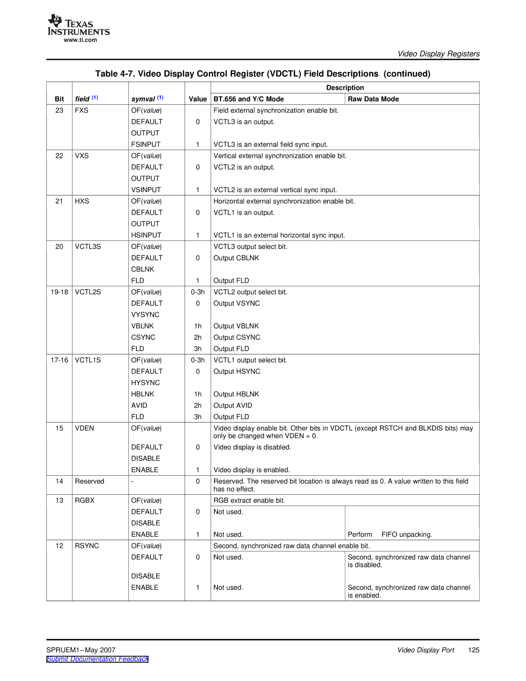
| Table | (continued) | ||||
|
|
|
| Description |
| |
Bit | field (1) | symval (1) | Value | BT.656 and Y/C Mode | Raw Data Mode | |
23 | FXS | OF(value) |
| Field external synchronization enable bit. |
|
|
|
| DEFAULT | 0 | VCTL3 is an output. |
|
|
|
| OUTPUT |
|
|
|
|
|
| FSINPUT | 1 | VCTL3 is an external field sync input. |
|
|
22 | VXS | OF(value) |
| Vertical external synchronization enable bit. |
|
|
|
| DEFAULT | 0 | VCTL2 is an output. |
|
|
|
| OUTPUT |
|
|
|
|
|
| VSINPUT | 1 | VCTL2 is an external vertical sync input. |
|
|
21 | HXS | OF(value) |
| Horizontal external synchronization enable bit. |
| |
|
| DEFAULT | 0 | VCTL1 is an output. |
|
|
|
| OUTPUT |
|
|
|
|
|
| HSINPUT | 1 | VCTL1 is an external horizontal sync input. |
|
|
20 | VCTL3S | OF(value) |
| VCTL3 output select bit. |
|
|
|
| DEFAULT | 0 | Output CBLNK |
|
|
|
| CBLNK |
|
|
|
|
|
| FLD | 1 | Output FLD |
|
|
VCTL2S | OF(value) | VCTL2 output select bit. |
|
| ||
|
| DEFAULT | 0 | Output VSYNC |
|
|
|
| VYSYNC |
|
|
|
|
|
| VBLNK | 1h | Output VBLNK |
|
|
|
| CSYNC | 2h | Output CSYNC |
|
|
|
| FLD | 3h | Output FLD |
|
|
VCTL1S | OF(value) | VCTL1 output select bit. |
|
| ||
|
| DEFAULT | 0 | Output HSYNC |
|
|
|
| HYSYNC |
|
|
|
|
|
| HBLNK | 1h | Output HBLNK |
|
|
|
| AVID | 2h | Output AVID |
|
|
|
| FLD | 3h | Output FLD |
|
|
15 | VDEN | OF(value) |
| Video display enable bit. Other bits in VDCTL (except RSTCH and BLKDIS bits) may | ||
|
|
|
| only be changed when VDEN = 0. |
|
|
|
| DEFAULT | 0 | Video display is disabled. |
|
|
|
| DISABLE |
|
|
|
|
|
| ENABLE | 1 | Video display is enabled. |
|
|
14 | Reserved | - | 0 | Reserved. The reserved bit location is always read as 0. A value written to this field | ||
|
|
|
| has no effect. |
|
|
13 | RGBX | OF(value) |
| RGB extract enable bit. |
|
|
|
| DEFAULT | 0 | Not used. |
|
|
|
| DISABLE |
|
|
|
|
|
| ENABLE | 1 | Not used. | Perform | FIFO unpacking. |
12 | RSYNC | OF(value) |
| Second, synchronized raw data channel enable bit. |
| |
|
| DEFAULT | 0 | Not used. | Second, synchronized raw data channel | |
|
|
|
|
| is disabled. | |
|
| DISABLE |
|
|
|
|
|
| ENABLE | 1 | Not used. | Second, synchronized raw data channel | |
|
|
|
|
| is enabled. |
|
SPRUEM1 | Video Display Port | 125 |
Submit Documentation Feedback |
|
|