www.ti.com
GPIO Registers
5.1GPIO Registers
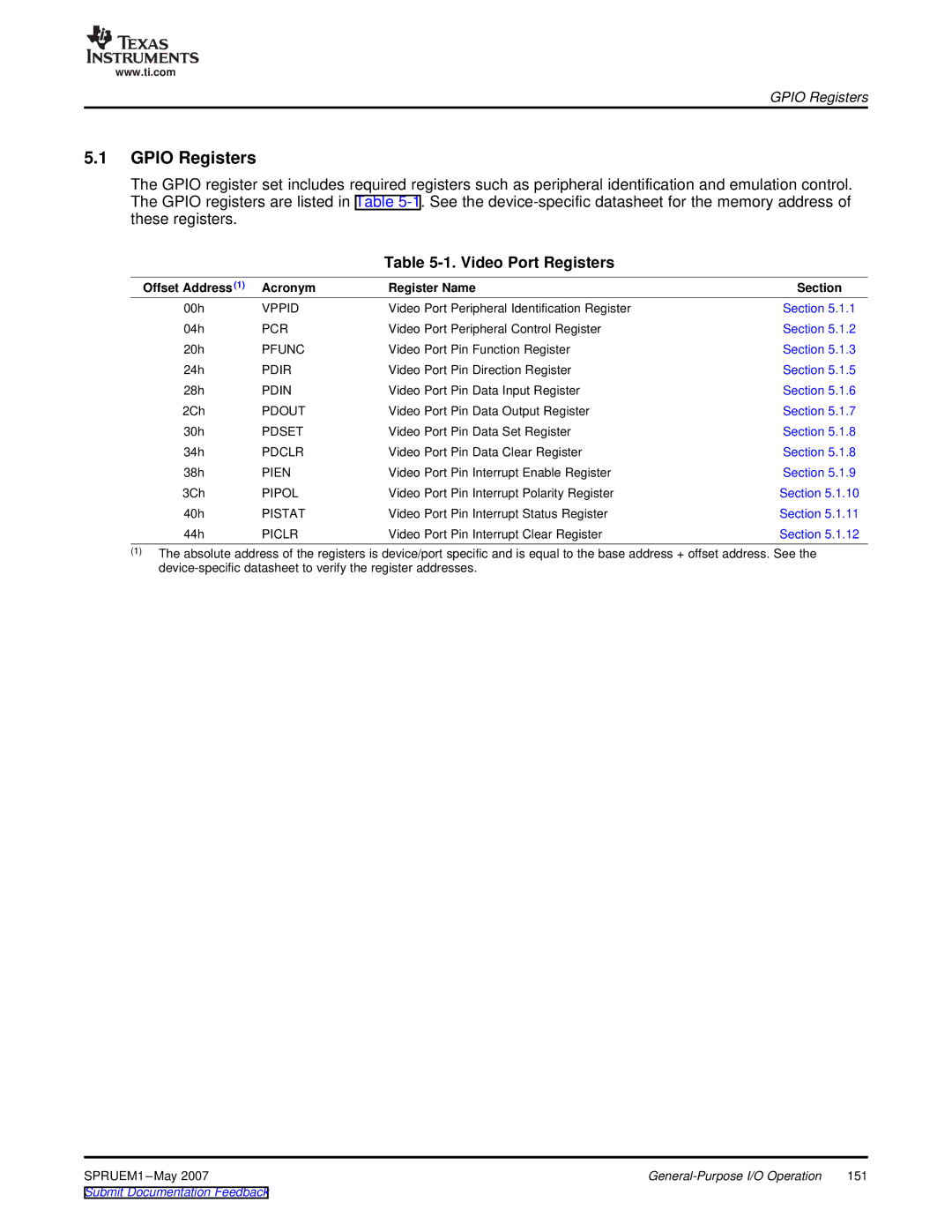
The GPIO register set includes required registers such as peripheral identification and emulation control. The GPIO registers are listed in Table
Table 5-1. Video Port Registers
Offset Address (1) | Acronym | Register Name | Section |
00h | VPPID | Video Port Peripheral Identification Register | Section 5.1.1 |
04h | PCR | Video Port Peripheral Control Register | Section 5.1.2 |
20h | PFUNC | Video Port Pin Function Register | Section 5.1.3 |
24h | PDIR | Video Port Pin Direction Register | Section 5.1.5 |
28h | PDIN | Video Port Pin Data Input Register | Section 5.1.6 |
2Ch | PDOUT | Video Port Pin Data Output Register | Section 5.1.7 |
30h | PDSET | Video Port Pin Data Set Register | Section 5.1.8 |
34h | PDCLR | Video Port Pin Data Clear Register | Section 5.1.8 |
38h | PIEN | Video Port Pin Interrupt Enable Register | Section 5.1.9 |
3Ch | PIPOL | Video Port Pin Interrupt Polarity Register | Section 5.1.10 |
40h | PISTAT | Video Port Pin Interrupt Status Register | Section 5.1.11 |
44h | PICLR | Video Port Pin Interrupt Clear Register | Section 5.1.12 |
(1)The absolute address of the registers is device/port specific and is equal to the base address + offset address. See the
SPRUEM1 | 151 | |
Submit Documentation Feedback |
|
|
