www.ti.com
Video Display Registers
Table
(continued)
|
|
| Description |
Bit field (1) | symval (1) | Value BT.656 and Y/C Mode | Raw Data Mode |
| where VBLNK active edge occurs for |
| field 2. |
Specifies the pixel (in FPCOUNT) where vertical blanking begins (VBLNK active edge) for field 2.
DEFAULT0
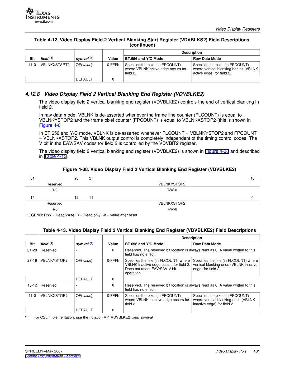
4.12.8 Video Display Field 2 Vertical Blanking End Register (VDVBLKE2)
The video display field 2 vertical blanking end register (VDVBLKE2) controls the end of vertical blanking in field 2.
In raw data mode, VBLNK is
In BT.656 and Y/C mode, VBLNK is
=VBLNKXSTOP2. This VBLNK output control is completely independent of the timing control codes. The V bit in the EAV/SAV codes for field 2 is controlled by the VDVBIT2 register.
The video display field 2 vertical blanking end register (VDVBLKE2) is shown in Figure
Figure 4-38. Video Display Field 2 Vertical Blanking End Register (VDVBLKE2)
31 | 28 | 27 | 16 |
| Reserved |
| VBLNKYSTOP2 |
|
| ||
15 | 12 | 11 | 0 |
| Reserved |
| VBLNKXSTOP2 |
|
|
LEGEND: R/W = Read/Write; R = Read only;
Table
|
|
|
|
| Description |
Bit | field (1) | symval (1) | Value | BT.656 and Y/C Mode | Raw Data Mode |
Reserved | - | 0 | Reserved. The reserved bit location is always read as 0. A value written to this | ||
|
|
|
| field has no effect. |
|
OF(value) | ||
|
| VBLNK inactive edge occurs for field 2. |
|
| Does not affect EAV/SAV V bit |
|
| operation. |
Specifies the line (in FLCOUNT) where vertical blanking ends (VBLNK inactive edge) for field 2.
| DEFAULT | 0 |
|
- | 0 | Reserved. The reserved bit location is always read as 0. A value written to this | |
|
|
| field has no effect. |
OF(value) | ||
|
| where VBLNK inactive edge occurs for |
|
| field 2. |
| DEFAULT | 0 |
(1)For CSL implementation, use the notation VP_VDVBLKE2_field_symval
Specifies the pixel (in FPCOUNT) where vertical blanking ends (VBLNK inactive edge) for field 2.
SPRUEM1 | Video Display Port | 131 |
Submit Documentation Feedback |
|
|