www.ti.com
Video Display Registers
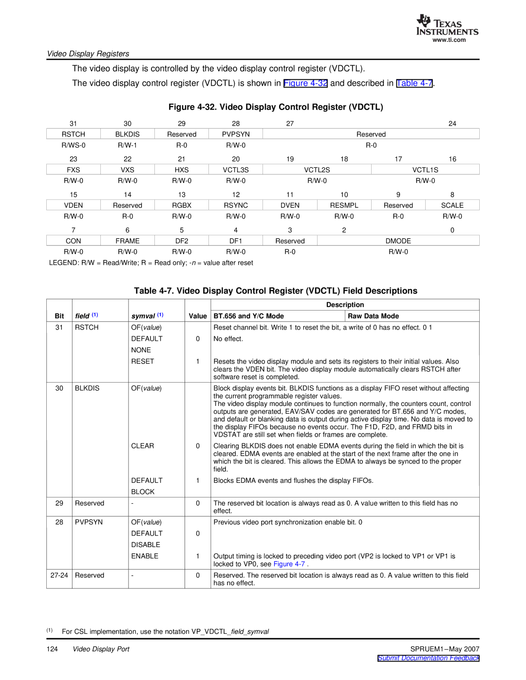
The video display is controlled by the video display control register (VDCTL).
The video display control register (VDCTL) is shown in Figure
Figure 4-32. Video Display Control Register (VDCTL)
31 | 30 | 29 | 28 | 27 |
|
| 24 |
RSTCH | BLKDIS | Reserved | PVPSYN |
| Reserved |
| |
|
|
| |||||
23 | 22 | 21 | 20 | 19 | 18 | 17 | 16 |
FXS | VXS | HXS | VCTL3S | VCTL2S |
| VCTL1S |
|
|
| ||||||
15 | 14 | 13 | 12 | 11 | 10 | 9 | 8 |
VDEN | Reserved | RGBX | RSYNC | DVEN | RESMPL | Reserved | SCALE |
7 | 6 | 5 | 4 | 3 | 2 |
| 0 |
CON | FRAME | DF2 | DF1 | Reserved |
| DMODE |
|
|
| ||||||
LEGEND: R/W = Read/Write; R = Read only;
Table 4-7. Video Display Control Register (VDCTL) Field Descriptions
|
|
|
|
| Description |
Bit | field (1) | symval (1) | Value | BT.656 and Y/C Mode | Raw Data Mode |
31 | RSTCH | OF(value) |
| Reset channel bit. Write 1 to reset the bit, a write of 0 has no effect. 0 1 | |
|
| DEFAULT | 0 | No effect. |
|
|
| NONE |
|
|
|
|
| RESET | 1 | Resets the video display module and sets its registers to their initial values. Also | |
|
|
|
| clears the VDEN bit. The video display module automatically clears RSTCH after | |
|
|
|
| software reset is completed. |
|
30 | BLKDIS | OF(value) |
| Block display events bit. BLKDIS functions as a display FIFO reset without affecting | |
|
|
|
| the current programmable register values. | |
|
|
|
| The video display module continues to function normally, the counters count, control | |
|
|
|
| outputs are generated, EAV/SAV codes are generated for BT.656 and Y/C modes, | |
|
|
|
| and default or blanking data is output during active display time. No data is moved to | |
|
|
|
| the display FIFOs because no events occur. The F1D, F2D, and FRMD bits in | |
|
|
|
| VDSTAT are still set when fields or frames are complete. | |
|
| CLEAR | 0 | Clearing BLKDIS does not enable EDMA events during the field in which the bit is | |
|
|
|
| cleared. EDMA events are enabled at the start of the next frame after the one in | |
|
|
|
| which the bit is cleared. This allows the EDMA to always be synced to the proper | |
|
|
|
| field. |
|
|
| DEFAULT | 1 | Blocks EDMA events and flushes the display FIFOs. | |
|
| BLOCK |
|
|
|
29 | Reserved | - | 0 | The reserved bit location is always read as 0. A value written to this field has no | |
|
|
|
| effect. |
|
28 | PVPSYN | OF(value) |
| Previous video port synchronization enable bit. 0 | |
|
| DEFAULT | 0 |
|
|
|
| DISABLE |
|
|
|
|
| ENABLE | 1 | Output timing is locked to preceding video port (VP2 is locked to VP1 or VP1 is | |
|
|
|
| locked to VP0, see Figure |
|
Reserved | - | 0 | Reserved. The reserved bit location is always read as 0. A value written to this field | ||
|
|
|
| has no effect. |
|
(1)For CSL implementation, use the notation VP_VDCTL_field_symval
124 | Video Display Port | SPRUEM1 |