www.ti.com
GPIO Registers
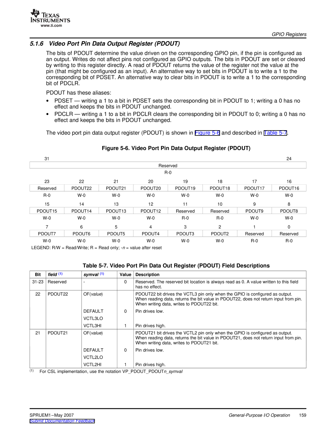
5.1.6 Video Port Pin Data Output Register (PDOUT)
The bits of PDOUT determine the value driven on the corresponding GPIO pin, if the pin is configured as an output. Writes do not affect pins not configured as GPIO outputs. The bits in PDOUT are set or cleared by writing to this register directly. A read of PDOUT returns the value of the register not the value at the pin (that might be configured as an input). An alternative way to set bits in PDOUT is to write a 1 to the corresponding bit of PDSET. An alternative way to clear bits in PDOUT is to write a 1 to the corresponding bit of PDCLR.
PDOUT has these aliases:
∙PDSET — writing a 1 to a bit in PDSET sets the corresponding bit in PDOUT to 1; writing a 0 has no effect and keeps the bits in PDOUT unchanged.
∙PDCLR — writing a 1 to a bit in PDCLR clears the corresponding bit in PDOUT to 0; writing a 0 has no effect and keeps the bits in PDOUT unchanged.
The video port pin data output register (PDOUT) is shown in Figure
Figure 5-6. Video Port Pin Data Output Register (PDOUT)
31 |
|
|
|
|
|
| 24 |
|
|
| Reserved |
|
|
| |
|
|
|
|
|
|
| |
23 | 22 | 21 | 20 | 19 | 18 | 17 | 16 |
Reserved | PDOUT22 | PDOUT21 | PDOUT20 | PDOUT19 | PDOUT18 | PDOUT17 | PDOUT16 |
15 | 14 | 13 | 12 | 11 | 10 | 9 | 8 |
PDOUT15 | PDOUT14 | PDOUT13 | PDOUT12 | Reserved | Reserved | PDOUT9 | PDOUT8 |
7 | 6 | 5 | 4 | 3 | 2 | 1 | 0 |
PDOUT7 | PDOUT6 | PDOUT5 | PDOUT4 | PDOUT3 | PDOUT2 | Reserved | Reserved |
LEGEND: R/W = Read/Write; R = Read only;
Table 5-7. Video Port Pin Data Out Register (PDOUT) Field Descriptions
Bit | field (1) | symval (1) | Value | Description |
Reserved | - | 0 | Reserved. The reserved bit location is always read as 0. A value written to this field | |
|
|
|
| has no effect. |
22 | PDOUT22 | OF(value) |
| PDOUT22 bit drives the VCTL3 pin only when the GPIO is configured as output. |
|
|
|
| When reading data, returns the bit value in PDOUT22, does not return input from pin. |
|
|
|
| When writing data, writes to PDOUT22 bit. |
|
| DEFAULT | 0 | Pin drives low. |
|
| VCTL3LO |
|
|
|
| VCTL3HI | 1 | Pin drives high. |
21 | PDOUT21 | OF(value) |
| PDOUT21 bit drives the VCTL2 pin only when the GPIO is configured as output. |
|
|
|
| When reading data, returns the bit value in PDOUT21, does not return input from pin. |
|
|
|
| When writing data, writes to PDOUT21 bit. |
|
| DEFAULT | 0 | Pin drives low. |
|
| VCTL2LO |
|
|
|
| VCTL2HI | 1 | Pin drives high. |
(1)For CSL implementation, use the notation VP_PDOUT_PDOUTn_symval
SPRUEM1 | 159 | |
Submit Documentation Feedback |
|
|