Texas Instruments TMS320DM648 manual Sync Signal Generation, External Sync Operation

Models: TMS320DM648

1 174
Download 174 pages 10.69 Kb
Page 98
Image 98

www.ti.com

BT.656 Video Display Mode

4.1.3 Sync Signal Generation

The video display module must generate a number of control signals for both internal and external use. As seen in Section 4.1.2, the HSYNC, HBLNK, VSYNC, VBLNK, and FLD signals are generated directly from the pixel and line counters and comparison registers. Several additional signals are also generated indirectly for use in external control.

A composite blank (CBLNK) signal is generated as the logical-OR of the HBLNK and VBLNK signals. A composite sync (CSYNC) signal is also generated as the logical-OR of the HSYNC and VSYNC signals. (This is not a true analog CSYNC, which must include serration pulses during VSYNC and equalization pulses during vertical front and back porch periods.) Finally, an active video (AVID) signal is generated. AVID is the inverted CBLNK signal indicating when active video data is being output.

Up to three of the eight sync signals may be output on VCTL1, VCTL2, and VCTL3 as selected by the video display control register (VDCTL). Each signal may be output in its non-inverted or inverted form, as selected by the VCTnP bits in the video port control register (VPCTL).

4.1.4 External Sync Operation

The video display module may be synchronized with an external video source using external sync signals. VCTL1 may be configured as an external horizontal sync input. When the external HSYNC is asserted, FPCOUNT is loaded with the HRLD value and VCCOUNT is loaded with the CRLD value. VCTL2 may be configured as an external vertical sync input. When the external VSYNC is asserted during field 1, FLCOUNT is loaded with the VRLD value. Field determination is made using either VCTL3 as an external FLD input or by field detect logic using the VSYNC and HSYNC inputs.

4.1.5 Port Sync Operation

The video display module may be synchronized with the video display module of another video port on the device. This mode is provided to enable the output of 24-bit RGB data (for example, 8 bits of R and 8 bits of G on video port 0 operating in dual-channel synched 8-bit raw mode, and 8 bits of B on video port 1 operating in 8-bit raw mode with VP1 synched to VP0.) The slave port must have the same VCLKIN and programmed register values as the master port. The master port provides the control signals necessary to reset the slave port counters so that they maintain synchronization. Each video port may only synchronize to the previous videoport(the one with a lower number). An example for a three port device is shown in Figure 4-7.

Figure 4-7. Video Display Module Synchronization Chain

Video port 0

display

Can sync to

Video port 1

display

Can sync to

Video port 2

display

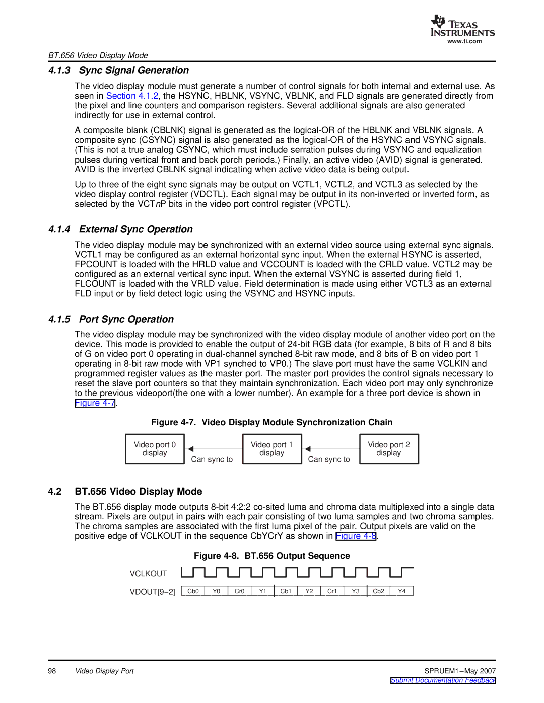
4.2BT.656 Video Display Mode

The BT.656 display mode outputs 8-bit 4:2:2 co-sited luma and chroma data multiplexed into a single data stream. Pixels are output in pairs with each pair consisting of two luma samples and two chroma samples. The chroma samples are associated with the first luma pixel of the pair. Output pixels are valid on the positive edge of VCLKOUT in the sequence CbYCrY as shown in Figure 4-8.

Figure 4-8. BT.656 Output Sequence

VCLKOUT

VDOUT[9−2]

Cb0

Y0

Cr0

Y1

Cb1

Y2

Cr1

Y3

Cb2

Y4

98

Video Display Port

SPRUEM1 –May 2007

Submit Documentation Feedback

Page 98
Image 98
Texas Instruments TMS320DM648 manual Sync Signal Generation, External Sync Operation, Port Sync Operation