www.ti.com
Video Port Registers
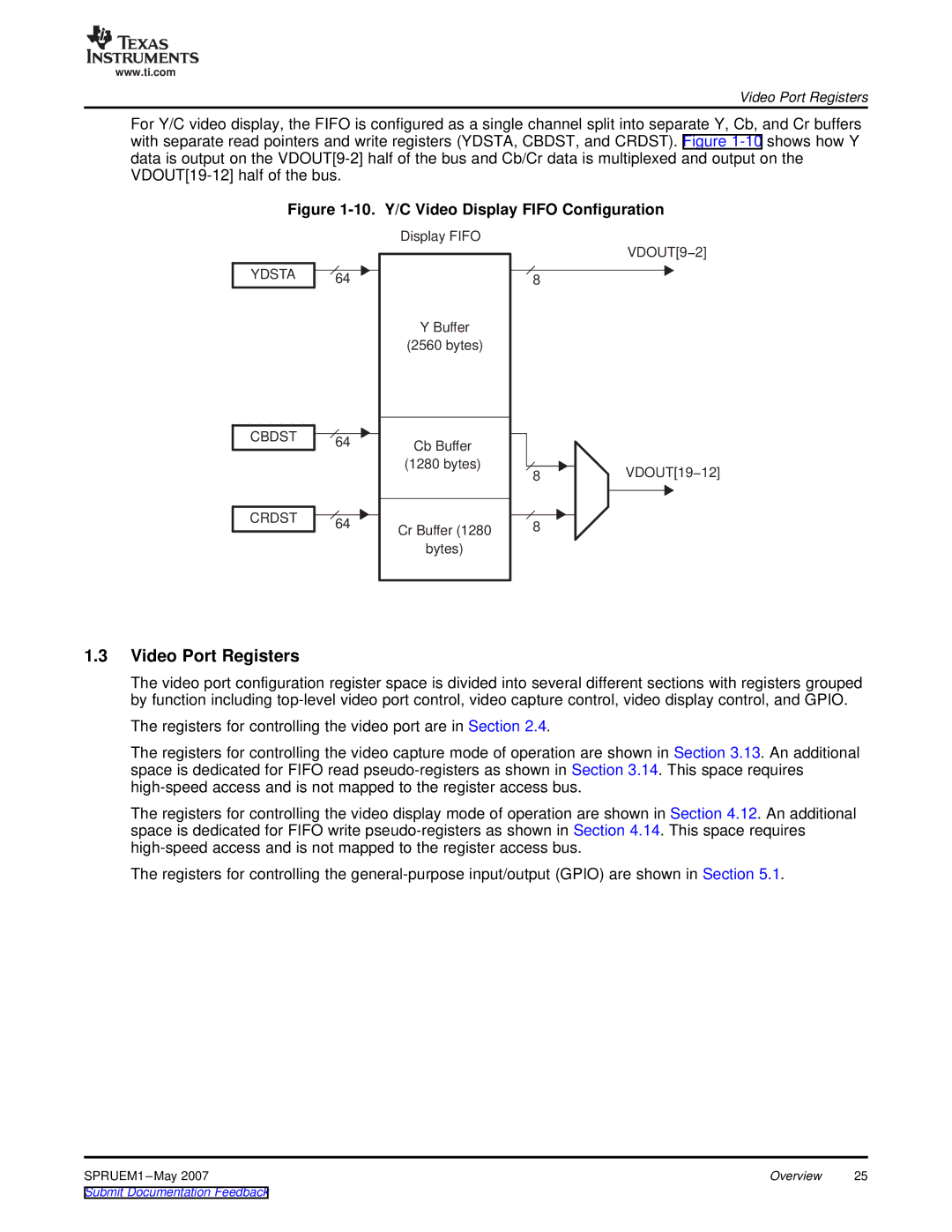
For Y/C video display, the FIFO is configured as a single channel split into separate Y, Cb, and Cr buffers with separate read pointers and write registers (YDSTA, CBDST, and CRDST). Figure
Figure 1-10. Y/C Video Display FIFO Configuration
YDSTA
CBDST
CRDST
64
64
64
Display FIFO
YBuffer (2560 bytes)
Cb Buffer
(1280 bytes)
Cr Buffer (1280
bytes)
| VDOUT[9−2] |
8 |
|
8 | VDOUT[19−12] |
8 |
|
1.3Video Port Registers
The video port configuration register space is divided into several different sections with registers grouped by function including
The registers for controlling the video port are in Section 2.4.
The registers for controlling the video capture mode of operation are shown in Section 3.13. An additional space is dedicated for FIFO read
The registers for controlling the video display mode of operation are shown in Section 4.12. An additional space is dedicated for FIFO write
The registers for controlling the
SPRUEM1 | Overview | 25 |