www.ti.com
Video Display FIFO Registers
4.14 Video Display FIFO Registers
The display FIFO mapping registers are listed in Table
The function of the video display FIFO mapping registers is listed in Table
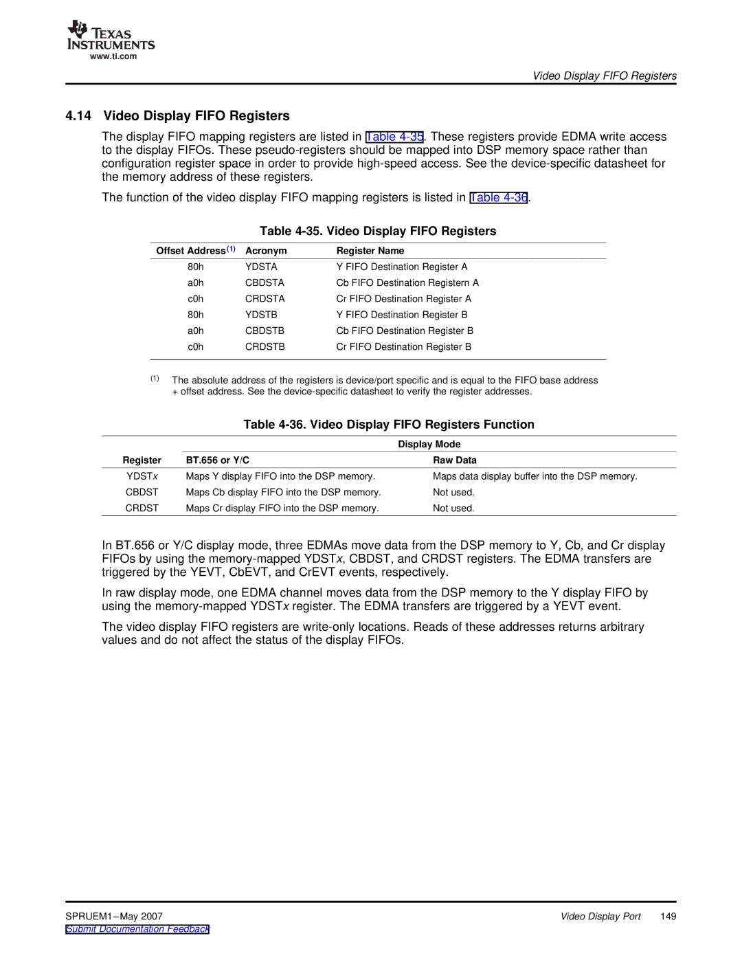
Table 4-35. Video Display FIFO Registers
Offset Address (1) | Acronym | Register Name |
80h | YDSTA | Y FIFO Destination Register A |
a0h | CBDSTA | Cb FIFO Destination Registern A |
c0h | CRDSTA | Cr FIFO Destination Register A |
80h | YDSTB | Y FIFO Destination Register B |
a0h | CBDSTB | Cb FIFO Destination Register B |
c0h | CRDSTB | Cr FIFO Destination Register B |
(1)The absolute address of the registers is device/port specific and is equal to the FIFO base address + offset address. See the
Table 4-36. Video Display FIFO Registers Function
|
| Display Mode |
Register | BT.656 or Y/C | Raw Data |
YDSTx | Maps Y display FIFO into the DSP memory. | Maps data display buffer into the DSP memory. |
CBDST | Maps Cb display FIFO into the DSP memory. | Not used. |
CRDST | Maps Cr display FIFO into the DSP memory. | Not used. |
In BT.656 or Y/C display mode, three EDMAs move data from the DSP memory to Y, Cb, and Cr display FIFOs by using the
In raw display mode, one EDMA channel moves data from the DSP memory to the Y display FIFO by using the
The video display FIFO registers are
SPRUEM1 | Video Display Port | 149 |