www.ti.com
Video Display Registers
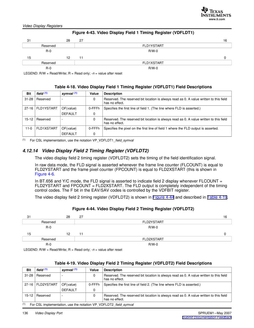
Figure 4-43. Video Display Field 1 Timing Register (VDFLDT1)
31 | 28 | 27 | 16 |
| Reserved |
| FLD1YSTART |
|
| ||
15 | 12 | 11 | 0 |
| Reserved |
| FLD1XSTART |
|
|
LEGEND: R/W = Read/Write; R = Read only;
Table
Bit | field (1) | symval (1) | Value | Description |
Reserved | - | 0 | Reserved. The reserved bit location is always read as 0. A value written to this field | |
|
|
|
| has no effect. |
FLD1YSTART | OF(value) | Specifies the first line of field 1. (The line where FLD is asserted.) | ||
|
| DEFAULT | 0 |
|
Reserved | - | 0 | Reserved. The reserved bit location is always read as 0. A value written to this field | |
|
|
|
| has no effect. |
FLD1XSTART | OF(value) | Specifies the pixel on the first line of field 1 where the FLD output is asserted. | ||
|
| DEFAULT | 0 |
|
(1)For CSL implementation, use the notation VP_VDFLDT1_field_symval
4.12.14 Video Display Field 2 Timing Register (VDFLDT2)
The video display field 2 timing register (VDFLDT2) sets the timing of the field identification signal.
In raw data mode, the FLD signal is asserted whenever the frame line counter (FLCOUNT) is equal to FLD2YSTART and the frame pixel counter (FPCOUNT) is equal to FLD2XSTART (this is shown in Figure
In BT.656 and Y/C mode, the FLD signal is asserted to indicate field 2 display whenever FLCOUNT = FLD2YSTART and FPCOUNT = FLD2XSTART. The FLD output is completely independent of the timing control codes. The F bit in the EAV/SAV codes is controlled by the VDFBIT register.
The video display field 2 timing register (VDFLDT2) is shown in Figure
Figure 4-44. Video Display Field 2 Timing Register (VDFLDT2)
31 | 28 | 27 | 16 |
| Reserved |
| FLD2YSTART |
|
| ||
15 | 12 | 11 | 0 |
| Reserved |
| FLD2XSTART |
|
|
LEGEND: R/W = Read/Write; R = Read only;
Table
Bit | field (1) | symval (1) | Value | Description |
Reserved | - | 0 | Reserved. The reserved bit location is always read as 0. A value written to this field | |
|
|
|
| has no effect. |
FLD2YSTART | OF(value) | Specifies the first line of field 2. (The line where FLD is asserted.) | ||
|
| DEFAULT | 0 |
|
Reserved | - | 0 | Reserved. The reserved bit location is always read as 0. A value written to this field | |
|
|
|
| has no effect. |
(1)For CSL implementation, use the notation VP_VDFLDT2_field_symval
136 | Video Display Port | SPRUEM1 |