www.ti.com
|
|
|
|
|
| Video Display Registers |
|
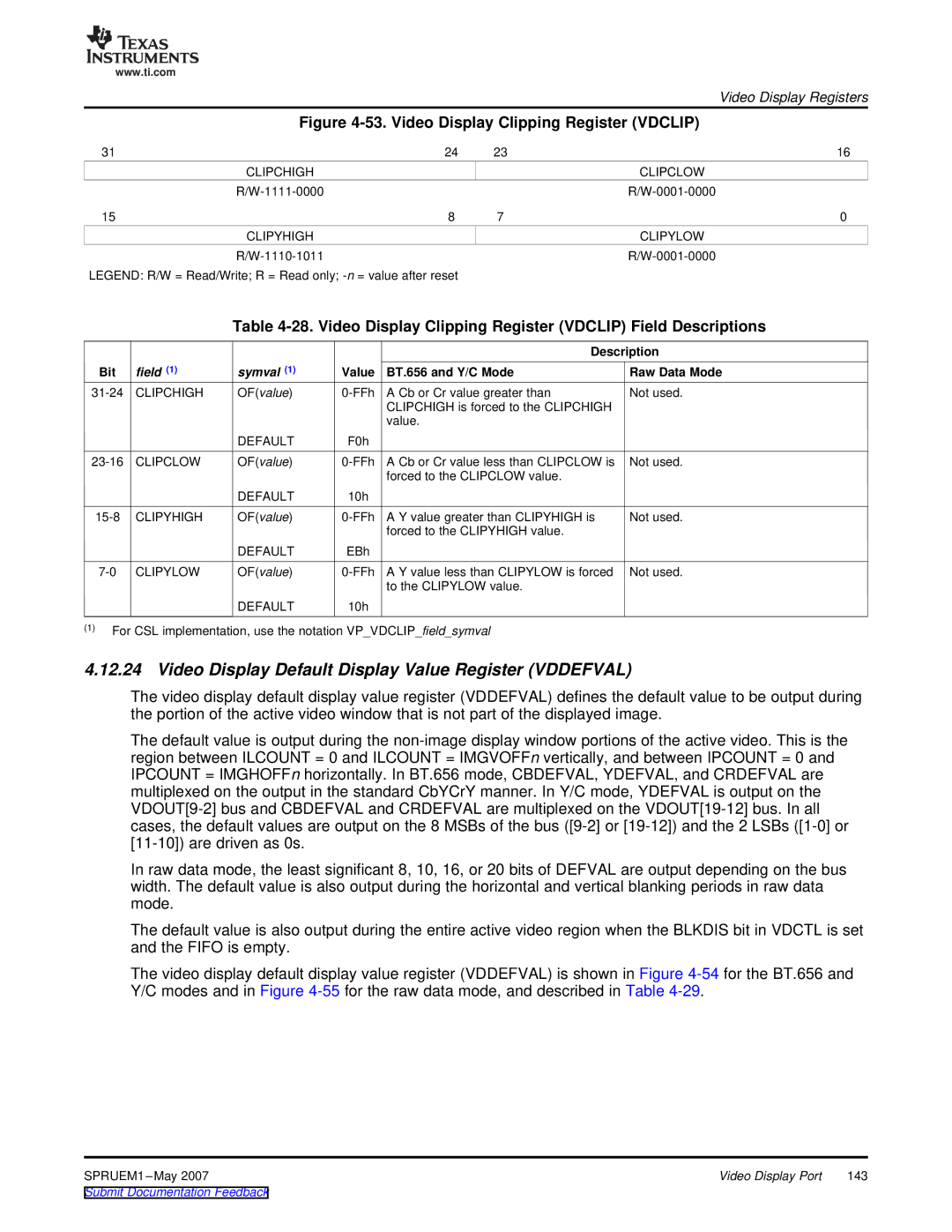
| Figure | ||||
31 |
|
|
| 24 | 23 | 16 |
|
| CLIPCHIGH |
|
|
| CLIPCLOW |
|
|
|
|
| ||
15 |
|
|
| 8 | 7 | 0 |
|
| CLIPYHIGH |
|
|
| CLIPYLOW |
|
|
|
|
| ||
LEGEND: R/W = Read/Write; R = Read only; |
|
| ||||
|
| Table | ||||
|
|
|
|
| Description | |
Bit | field (1) | symval (1) | Value | BT.656 and Y/C Mode | Raw Data Mode | |
CLIPCHIGH | OF(value) | A Cb or Cr value greater than | Not used. | |||
|
|
|
| CLIPCHIGH is forced to the CLIPCHIGH |
| |
|
|
|
| value. |
|
|
|
| DEFAULT | F0h |
|
|
|
CLIPCLOW | OF(value) | A Cb or Cr value less than CLIPCLOW is | Not used. | |||
|
|
|
| forced to the CLIPCLOW value. |
| |
|
| DEFAULT | 10h |
|
|
|
CLIPYHIGH | OF(value) | A Y value greater than CLIPYHIGH is | Not used. | |||
|
|
|
| forced to the CLIPYHIGH value. |
| |
|
| DEFAULT | EBh |
|
|
|
CLIPYLOW | OF(value) | A Y value less than CLIPYLOW is forced | Not used. | |||
|
|
|
| to the CLIPYLOW value. |
| |
|
| DEFAULT | 10h |
|
|
|
(1)For CSL implementation, use the notation VP_VDCLIP_field_symval
4.12.24 Video Display Default Display Value Register (VDDEFVAL)
The video display default display value register (VDDEFVAL) defines the default value to be output during the portion of the active video window that is not part of the displayed image.
The default value is output during the
In raw data mode, the least significant 8, 10, 16, or 20 bits of DEFVAL are output depending on the bus width. The default value is also output during the horizontal and vertical blanking periods in raw data mode.
The default value is also output during the entire active video region when the BLKDIS bit in VDCTL is set and the FIFO is empty.
The video display default display value register (VDDEFVAL) is shown in Figure
SPRUEM1 | Video Display Port | 143 |