www.ti.com
GPIO Registers
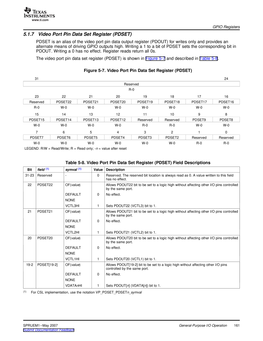
5.1.7 Video Port Pin Data Set Register (PDSET)
PDSET is an alias of the video port pin data output register (PDOUT) for writes only and provides an alternate means of driving GPIO outputs high. Writing a 1 to a bit of PDSET sets the corresponding bit in PDOUT. Writing a 0 has no effect. Register reads return all 0s.
The video port pin data set register (PDSET) is shown in Figure
Figure 5-7. Video Port Pin Data Set Register (PDSET)
31 |
|
|
|
|
|
| 24 |
|
|
| Reserved |
|
|
| |
|
|
|
|
|
|
| |
23 | 22 | 21 | 20 | 19 | 18 | 17 | 16 |
Reserved | PDSET22 | PDSET21 | PDSET20 | PDSET19 | PDSET18 | PDSET17 | PDSET16 |
15 | 14 | 13 | 12 | 11 | 10 | 9 | 8 |
PDSET15 | PDSET14 | PDSET13 | PDSET12 | Reserved | Reserved | PDSET9 | PDSET8 |
7 | 6 | 5 | 4 | 3 | 2 | 1 | 0 |
PDSET7 | PDSET6 | PDSET5 | PDSET4 | PDSET3 | PDSET2 | Reserved | Reserved |
LEGEND: R/W = Read/Write; R = Read only;
Table 5-8. Video Port Pin Data Set Register (PDSET) Field Descriptions
Bit | field (1) | symval (1) | Value | Description |
Reserved | - | 0 | Reserved. The reserved bit location is always read as 0. A value written to this field | |
|
|
|
| has no effect. |
22 | PDSET22 | OF(value) |
| Allows PDOUT22 bit to be set to a logic high without affecting other I/O pins controlled |
|
|
|
| by the same port. |
|
| DEFAULT | 0 | No effect. |
|
| NONE |
|
|
|
| VCTL3HI | 1 | Sets PDOUT22 (VCTL3) bit to 1. |
21 | PDSET21 | OF(value) |
| Allows PDOUT21 bit to be set to a logic high without affecting other I/O pins controlled |
|
|
|
| by the same port. |
|
| DEFAULT | 0 | No effect. |
|
| NONE |
|
|
|
| VCTL2HI | 1 | Sets PDOUT21 (VCTL2) bit to 1. |
20 | PDSET20 | OF(value) |
| Allows PDOUT20 bit to be set to a logic high without affecting other I/O pins controlled |
|
|
|
| by the same port. |
|
| DEFAULT | 0 | No effect. |
|
| NONE |
|
|
|
| VCTL1HI | 1 | Sets PDOUT20 (VCTL1) bit to 1. |
OF(value) |
| Allows | ||
|
|
|
| controlled by the same port. |
|
| DEFAULT | 0 | No effect. |
|
| NONE |
|
|
|
| VDATAnHI | 1 | Sets PDOUT[n] (VDATA[n]) bit to 1. |
(1)For CSL implementation, use the notation VP_PDSET_PDSETn_symval
SPRUEM1 | 161 | |
Submit Documentation Feedback |
|
|